
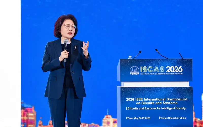
Huawei has introduced the Tau scaling law, a new semiconductor design methodology that replaces traditional exponential scaling with time-based scaling to improve performance and power efficiency across device levels.
New time-based methodology replaces exponential growth for better efficiency.
The company also unveiled the LogicFolding architecture at the circuit level, which shortens critical path wiring to reduce signal propagation resistance and capacitance. This approach aims to break physical boundaries of existing layouts while increasing transistor density and overall chip performance.
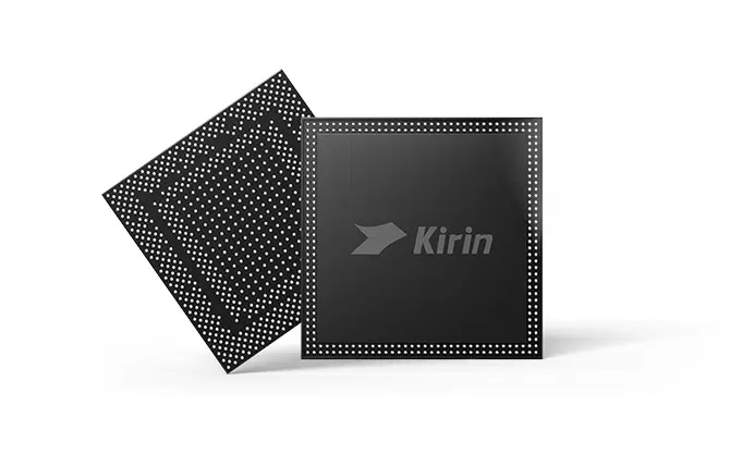
Huawei stated that it has designed and mass-produced 381 chips based on the Tau scaling law over the past six years. The company projects that its first Kirin chip utilizing the LogicFolding architecture will launch in Fall 2026, with a long-term goal of achieving 1.4nm equivalent transistor density by 2031.
A Huawei representative emphasized that openness and cooperation are essential for advancing the semiconductor industry. The vendor described the Tau scaling law as a framework for global collaboration among scientists, engineers, and industry partners to drive sustainable development in electronics manufacturing.


Discussion
0 comments
Log in to join the thread with a thoughtful take, question, or correction.