
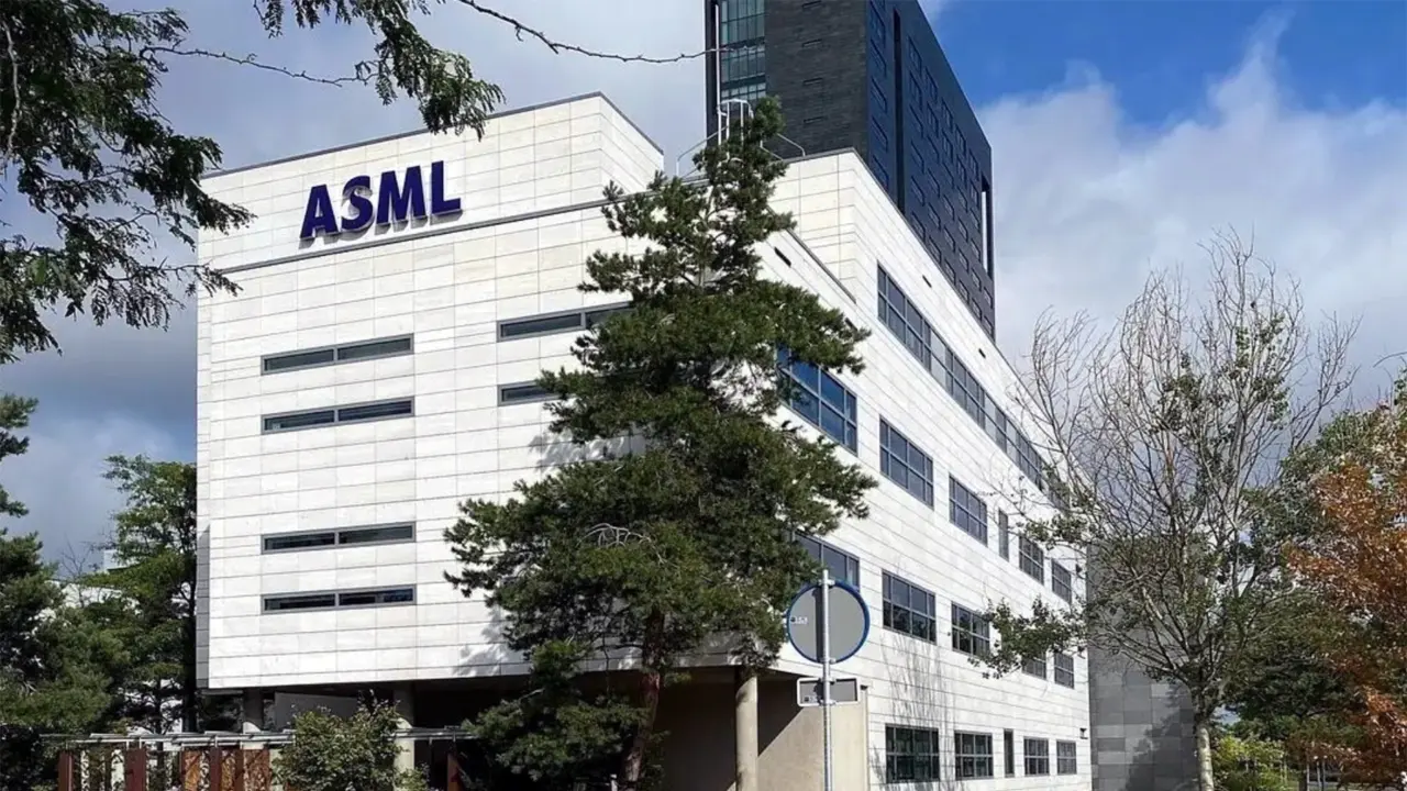
ASML is doubling down on its current laser-based approach for next-generation chipmaking tools, rejecting an alternative method that has drawn attention from industry outsiders. This strategic choice matters because it confirms that the semiconductor industry will rely on proven laser-produced plasma technology for the foreseeable future rather than shifting to more complex particle accelerator systems. Buyers and manufacturers can expect continued investment in refining existing EUV scanners instead of waiting for a disruptive new light source architecture.
ASML confirms 1,000W laser plasma target while dismissing particle accelerator alternative
The company's EUV lithography scanners use laser-produced plasma to generate the extreme ultraviolet light needed to etch microscopic circuits onto silicon wafers. ASML has steadily increased the power of these light sources from around 250W to approximately 500W in recent years. The firm now plans to push this power output to 1,000W in the coming years to boost manufacturing efficiency. This path relies on firing high-energy lasers at tin droplets to create the necessary plasma.
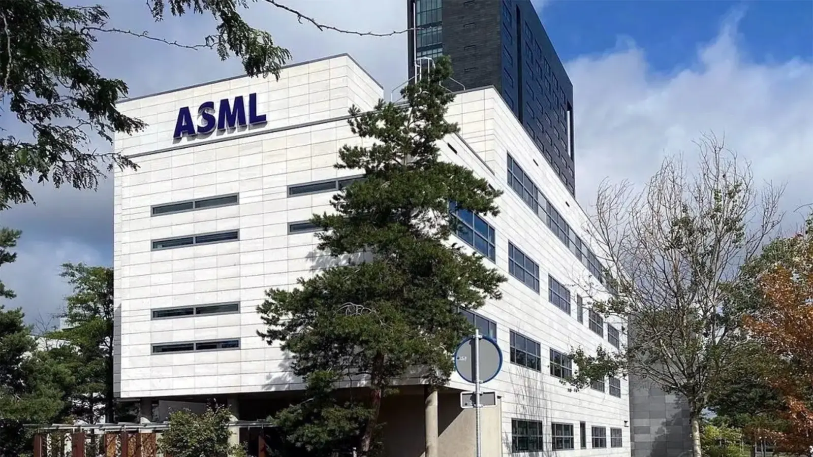
To support higher power levels, ASML intends to almost double the rate at which it generates tin droplets to 100,000 per second. The system emits 13.5-nm EUV radiation, which is the standard wavelength for current advanced node manufacturing. This approach requires precise management of debris and plasma stability, which the company has optimized over many years of development. The focus remains on scaling the existing laser-based infrastructure rather than building entirely new facilities.
An alternative technology known as Free-Electron Laser, or FEL, has been discussed as a potential future option for generating even higher EUV power. FEL systems eliminate the tin droplet debris problem inherent in laser-produced plasma but require complex particle accelerators and significant infrastructure changes. Industry analysis suggests that FEL technology will likely take a decade or more to rival laser-produced plasma in real semiconductor production facilities. ASML sees no immediate reason to adopt this method given the rapid advances in its current laser technology.
A JPMorgan note, as reported by Semi Doped, states that ASML sees no reason to try the new FEL light source favored by Elon Musk. This decision reinforces the company's commitment to its established supply chain and manufacturing processes. The semiconductor industry will continue to rely on ASML's laser-produced plasma systems for the next generation of chips. This confirmation provides clarity for manufacturers planning their long-term capital expenditure strategies.
Discussion
0 comments
Log in to join the thread with a thoughtful take, question, or correction.