
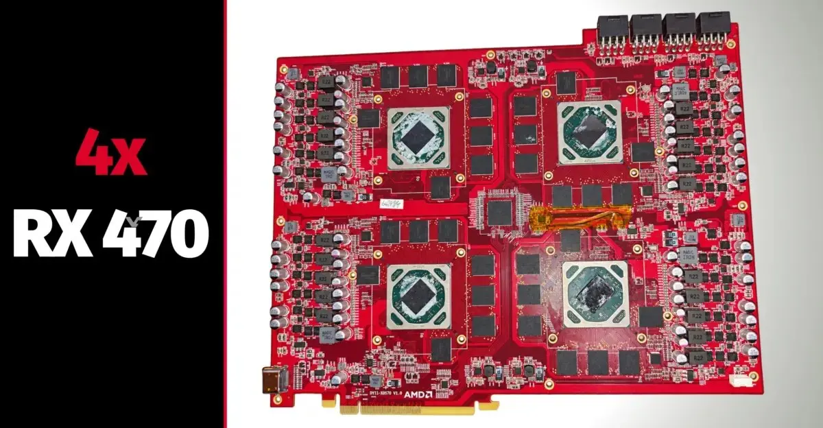
Hardware enthusiasts interested in mining history have something new to look at. A very rare prototype AMD PCB with 4 Radeon RX 470 GPUs has just been revealed online. It's a quad-GPU setup that is double the density of previous dual-GPU mining cards like Sapphire RX 570. This gives us tangible examples of what AMD was trying to do with high-density setups before going all-in on mass-production.
Rare PCB with 32GB GDDR5 memory surfaces online
This particular PCB marked as DYII-XQ570 V1.0 is labeled with an AMD logo. Images of this prototype have been shared by VideoCardz and leaker GOK. This is a 2×2 GPU package setup. Note it's not a regular x16 PCIe interface but x8.
Specifications
- GPU Configuration: Quad AMD Radeon RX 470 GPUs (2×2 configuration)
- Memory Capacity: 32GB GDDR5 total (8GB per GPU)
- Memory Chips: SK hynix H5GC8H24MJR (8Gb/1GB each)
- Power Connectors: Four 8-pin PCIe connectors
- PCIe Interface: PCIe x8
This quad-GPU board has up to 32GB GDDR5. It's 8GB of dedicated memory per RX 470 GPU. There are 4 of them, so overall there are 4 RX 470 GPUs on this board.
GDDR5 memory comes from SK hynix (H5GC8H24MJR). There is 1GB of storage per chip. There are 8 of them per GPU.
The board is powered via 4x 8-pin PCIe power. This x8 interface and no video ports clearly points to a specialized mining application. We haven't seen AMD release this specific quad-GPU Polaris board. This is simply an unannounced hardware discovery.
This is a unique experiment for GPU density. AMD is trying new things that go beyond normal consumer and even mining cards. This hasn't seen the light of day, for it to be commercially released. It's simply a piece of AMD hardware development history that we now have as a known prototype.
Four 8-pin connectors for a Polaris board seems excessive even for mining. The power delivery on those older chips was never that hungry.
wild that this never shipped tbh just a hardware museum piece at this point
Does anyone know if the x8 lane split causes bandwidth bottlenecks for the GDDR5 memory controllers on the RX 470 architecture?
The RX 470 memory bus is 256-bit. With four GPUs sharing an x8 link each, you are splitting the PCIe bandwidth per GPU, but the memory controllers are internal to each GPU. The bottleneck would be PCIe bandwidth to the host system, not the onboard memory.
This looks like a total waste of silicon. Why bundle four discrete dies when you could just make two faster chips?
32gb of VRAM for mining eth was a different era. Good times or bad times depending on who you ask lol
The article mentions this was never announced by AMD. The PCB marking suggests a third party OEM design that used AMD reference silicon rather than an official AMD board.
I suspect the thermal density on a 2×2 layout would be a nightmare without custom active cooling. Probably why it stayed a prototype.
Four 8-pin connectors is a lot of cables to manage.