
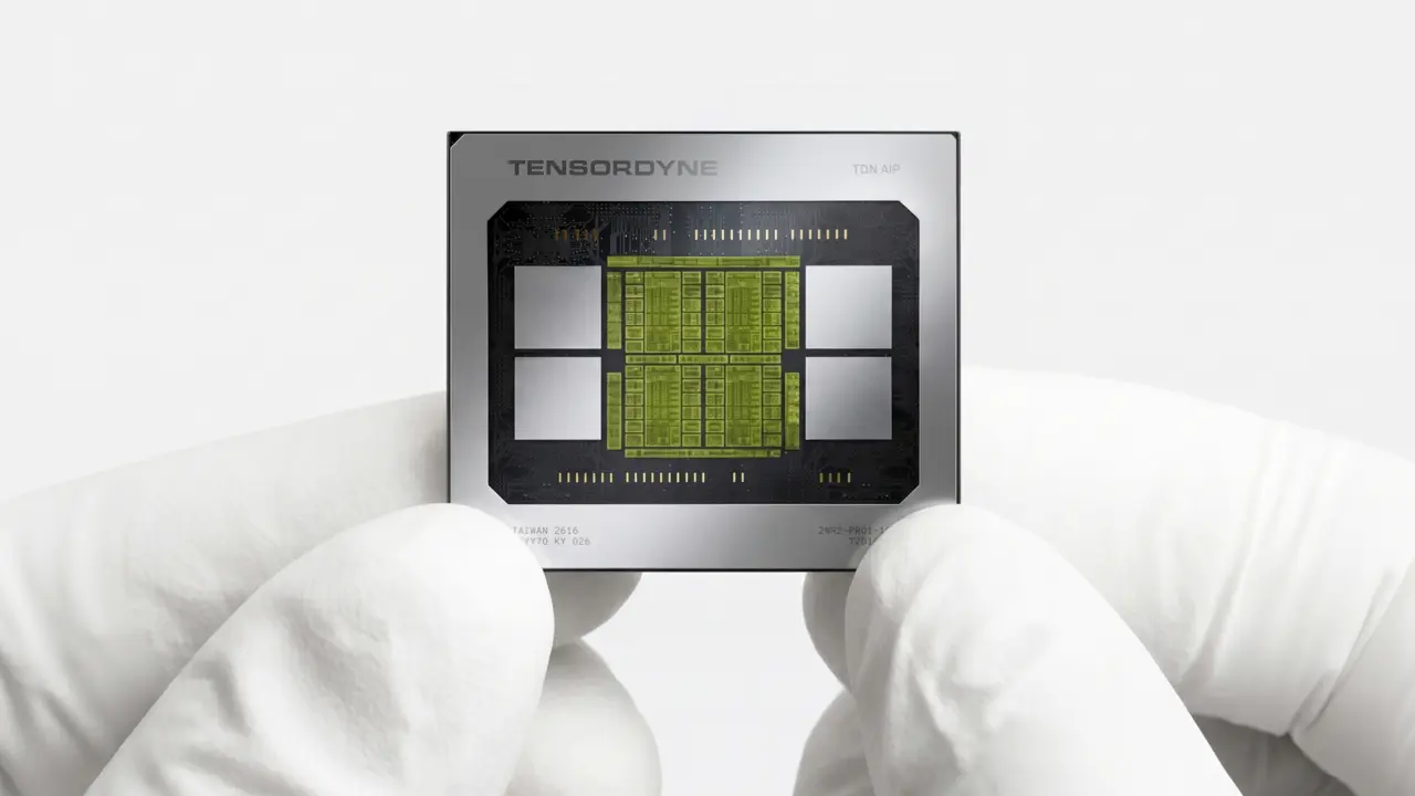
Tensordyne has announced the tape-out of Napier, its first AI accelerator built on TSMC’s 3nm process. The company claims this chip will deliver significantly higher token throughput and energy efficiency compared to NVIDIA Blackwell and Rubin architectures.
New 3nm accelerator targets large-scale inference workloads with logarithmic math architecture
The Napier TDN chip integrates 138 billion transistors into a single package. It pairs this compute density with 144 GB of HBM3E memory and 256 MB of SRAM to support large-scale AI inference workloads.
Napier Specifications
- Process Node: 3nm (TSMC)
- Transistor Count: 138 billion
- Memory Capacity: 144 GB HBM3E, 256 MB SRAM
- Peak Compute: 2.1 PFLOPs (Dense FP8)
- TDP: 300W

Performance projections from Tensordyne suggest the chip can achieve up to 2.1 PFLOPs of peak AI compute using Dense FP8 format. The system is designed with a logarithmic math architecture to handle multi-trillion parameter models at speeds exceeding 1000 tokens per second.
Tensordyne states that Napier offers 13 times higher token throughput and 17 times more tokens per watt than NVIDIA Blackwell. The company forecasts potential annual revenue gains of up to $33 million per rack compared to competing solutions.
The vendor is currently working toward a beta deployment phase for the platform. Tensordyne has also indicated strong market interest, forecasting over $200 million in demand for the Napier system upon release.



Discussion
0 comments
Log in to join the thread with a thoughtful take, question, or correction.