
Nagare Labs is introducing a new memory architecture called Z2RAM that could upend the way we’re currently layering memory in AI chips. The goal is to overcome the bandwidth problem which plagues processing speed today by delivering a SRAM speed with a DRAM density. It’s key because the approach is addressing key data transfer problems which are bottlenecks in AI today.
Capacitorless memory cell retains data for over 300 seconds at 85C in lab tests
Essentially, Z2RAM is based on this capacitorless 2T+ shield memory cell. This design eliminates the large capacitor in DRAM cells as we know them, enabling a much denser design. In fact, Nagare says Gen 1’s 6-layer stacking of these cells is what’s required to get the density they’re after.
Specifications
- Cell Architecture: Capacitorless, Two transistors and a shield
- Retention at 85°C: >300 seconds
- Gen 1 Density: 5x SRAM
- Gen 1 Speed: 14x DRAM
- Manufacturing Process: 7nm DUV lithography
These 3T cells in lab prototypes have greater than 300 sec retention at 85C. The Gen 1 projections show 5x the density of SRAM and 14x the speed of DRAM. They’re also aiming for 3x less energy than SRAM for reads. And they can do all of this using standard 7nm DUV litho (no need for EUV).
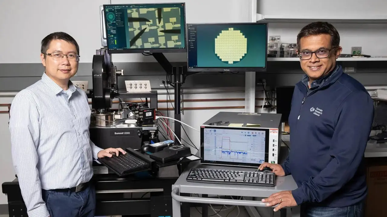
As co-founder Suman Datta put it, they’re literally in the prototype stage of lab development. They don’t have a fab today, but are looking for an R&D fab partner to help scale. The goal is to have Z2RAM tiles available for sampling in 4 years. And maybe the next decade for production shipments if they can get partners.

They claim 14x DRAM speed and 5x SRAM density. Does this mean we can finally stop using HBM in AI accelerators?
Not necessarily. They are targeting SRAM speed for on-chip caches and DRAM density for capacity. You still need high bandwidth for external memory. This is likely for tile-based stacking.
no capacitor is wild 🤔
300 seconds retention at 85C sounds good until you scale to six layers. Leakage will eat you alive. Lab prototypes are not products.
I just want to know if this makes enterprise servers cheaper. The price of RAM has been insane lately.
seven nanometer duv without euv is the real win here if it actually holds up.
The article says two transistors and a shield. That is a 3T cell. The headline text is confusing about the transistor count.
Great. Another layer of complexity for the fab partners. I bet the yield will be terrible for Gen 1.
If they can actually ship sampling in four years that would be a miracle. Most memory startups dissolve before the second prototype.