
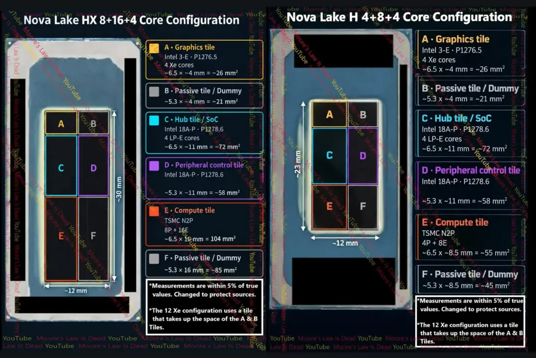
Intel has revealed the physical structure of their upcoming Nova Lake mobile processors for the next generation, giving us the first glimpse of the physical hardware inside the high-end laptops of the future. This reveal is significant as it shows that Intel is moving towards a complex multi-die architecture that will have a big impact on thermal and performance capabilities of the processors when fitted inside thin laptop bodies. It also gives both consumers and enthusiast a glimpse of what trade-offs Intel is making in the race to cram as many cores as possible inside their physical silicon footprint.
Intel reveals Nova Lake-HX and Nova Lake-H processor die specifications
For example, the top-tier Nova Lake-HX variant boasts an overall die area of 360mm2. Intel has gone with a huge package that leverages 4 different manufacturing processes to try to optimize performance and efficiency. They have chosen to distribute workload across multiple dies instead of one monolithic monolithic die. This allows them to leverage specific manufacturing processes for various sections of the processor.
Spec comparison
| Spec | Nova Lake-HX | Nova Lake-H |
|---|---|---|
| Core Configuration | 8P + 16E + 4LPE | 4P + 8E + 4LPE |
| Total Die Area | 360mm² | 276mm² |
| CPU Die Area | 104mm² | 55mm² |
| CPU Die Process | TSMC N2P | TSMC N2P |
| Passive Die Area | 85mm² | 45mm² |
To give you an idea, the Nova Lake-HX variant will feature 8 performance cores and 16 efficient cores, in addition to 4 low power efficient cores. The primary CPU die itself is 104mm2, based on TSMC N2P process node. Note that Intel has moved towards using third party manufacturing for the main CPU die this time around, which is a big change in their strategy.
The graphics processing unit itself is a separate die of 26mm2, based on Intel 3-E process. Finally, there is a dedicated 72mm2 die for low power tasks using the new Intel 18A-P process. Finally, the platform controller hub introduces another die of 58mm2 on the same 18A-P node. Finally, there is a passive die of 85mm2.
Intel has also shown us the smaller variant, known as Nova Lake-H, which caters to a slightly different audience of the mobile segment. This variant features 4P+8E+4LPE core configuration and has an overall die area of 276mm2. The CPU die for H variant is much smaller at 55mm2, also based on TSMC N2P.
The passive die in this case is smaller as well, at 45mm2 as this H variant has different thermal and power demands. So, you are getting a much smaller package that can fit in thinner laptops.
Rumor has it that Intel might switch to 4 digit names for their mobile chips in this case, following the desktop Core Ultra 4000 series. Such changes would make the new mobile architecture easier to differentiate from previous generations. We covered Intel Nova Lake Enters Qualification Stage in our earlier Intel coverage, where samples were already being tested for compatibility.
So, Intel has officially confirmed the physical specs and manufacturing partners for Nova Lake-HX and Nova Lake-H processors. A big change in the structure of mobile processors from Intel. This gives us a good benchmark with which to measure the performance and efficiency of upcoming hardware.


Discussion
0 comments
Log in to join the thread with a thoughtful take, question, or correction.