
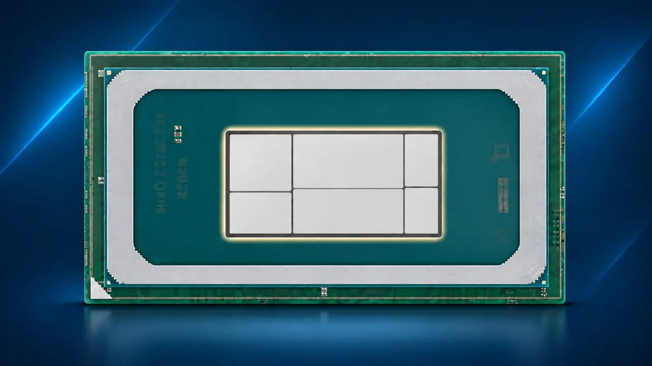
Intel going modular way with mobile processor design for more manufacturing flexibility. Based on leaked image of Nova Lake-H chip. We can clearly see a 6-tile design breaking up the monolithic die concept.
Leaked die shots show Intel Nova Lake-H uses a six-tile modular design with mixed manufacturing processes
This is the new modular design concept that will offer Intel to use different manufacturing process nodes for different tasks within a chip. This is a potential cost effective idea for laptop parts.
Nova Lake-H Specifications
- Tile Count: 6 tiles
- Compute Tile Size: 55 mm2
- Compute Tile Process: TSMC N2P
- Hub/SoC Tile Size: 72 mm2
- Hub/SoC Tile Process: Intel 18A-P
This leaked design mainly features Nova Lake-H (aka Core Ultra 4000H) processor. This is for the mainstream mobile market. It offers a mix of 4 Performance, 8 Efficiency, and 4 Low-Power E-cores.
This core layout is coupled with a dedicated graphics tile that will take care of integrated graphics workloads. It is all packed inside a 12 by 23 mm package. This is the physical size that laptop makers will use.
This modular chip architecture is going with 6-tiles TSMC N2P, Intel 18A-P, and Intel 3-E manufacturing processes. For fast computing tasks, a 55 sq. mm Compute Tile will go with TSMC’s high-end N2P process node. Another tile called Hub and SoC Tile (72 sq. mm) and Peripheral Controller Tile (58 sq. mm) will go with Intel’s 18A-P node. (The Hub/SoC Tile reportedly uses Intel’s 18A-P. Also, the Compute Tile will be on TSMC with N2P process.)
26 sq. mm graphics tile on Intel 3-E process node. Graphics Tile gets 4 cores for Xe3 GPU. There are two passive tiles for support structure in the chip. (That’s what leaks say.
Intel has not shared any official information about it.) Then there is the HX version of this chip that gets bigger 104 sq. mm Compute Tile. It will have 8P+16E cores.
We’re keeping a keen eye on the Intel Nova Lake-H. Check out the Intel Nova Lake-HX Die area hits. So, we have the leaked specifications of the Intel Nova Lake-H processor.
This processor (chip) is going with 6-tiles modular design. That’s the layout of the upcoming Intel Nova Lake-H and HX processors. Here we get the first look at the Nova Lake-H silicon (physical structure).



I see the 55 mm2 compute tile on TSMC N2P and the 72 mm2 hub tile on Intel 18A-P. Is the latency between these two process nodes actually managed well enough for gaming performance?
The die shot shows a dedicated peripheral controller tile at 58 mm2. That usually handles the interconnect bridge to keep latency low between the TSMC and Intel 18A-P sections.
six tiles for a laptop chip seems like overkill tbh 🤔
Leaks say 4P plus 8E plus 4 LPE cores. I suspect the efficiency cores will throttle hard under sustained load on these small tiles.
The graphics tile is only 26 mm2 with four Xe3 cores. That is going to be a bottleneck for anything modern.
I hope the modular design does not make repair costs insane when a single tile fails.
12 by 23 mm package is tiny. Thermal density must be a nightmare for the laptop OEMs 👀