
Chip designers targeting advanced process nodes now have a new domestic option for 3D integrated circuit (3DIC) physical design. Hejian Gongruan released two specialized software tools on September 1, 2024, to address a gap in the local market. These products aim to support logic folding and Tao's Law technical routes, which are critical for next-generation chip manufacturing. This launch provides local engineers with commercial-grade alternatives to traditional 2D design limitations.
New software tools target native 3D design and AI verification
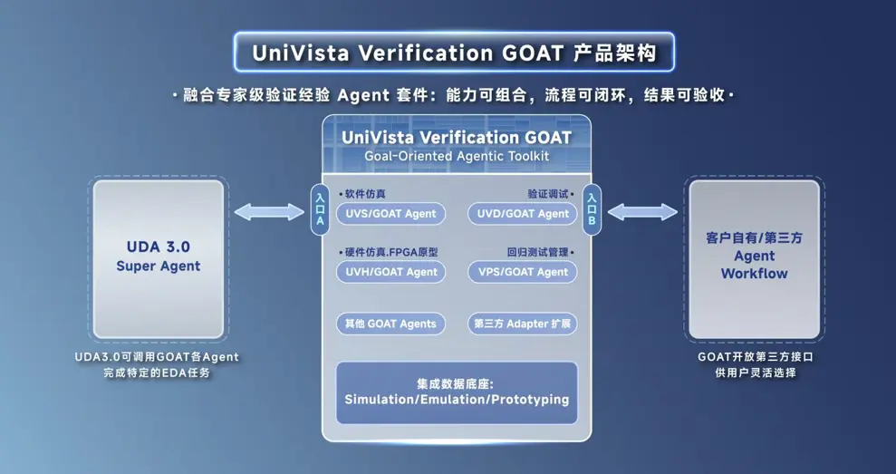
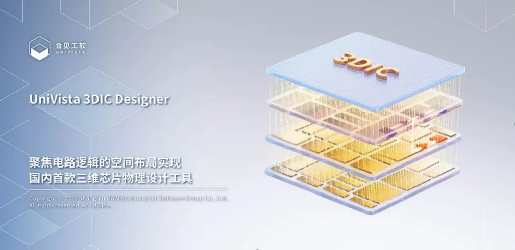
The first product is the UniVista 3DIC Designer, which serves as a physical design tool for 3DIC chips. The second offering is UniVista Verification GOAT, an AI agent suite designed for digital chip verification. Hejian Gongruan describes the verification suite as the first domestic Agentic EDA intelligent body strategy system. These tools target the specific needs of domestic advanced process nodes.
Current mainstream 3D packaging EDA solutions on the market are extensions of traditional 2.5D planar tools. They typically handle coarse-grained chiplet layered stacking for scenarios involving chiplets, interposers, silicon bridges, and HBM integration. Hejian Gongruan states that these existing tools cannot achieve unit-level native 3D global collaboration required for logic folding. The company claims its new software breaks the physical limits of traditional 2D chip design in performance, power consumption, and area.
He Peixin, CTO of Hejian Gongruan, explained that the core value of AI in EDA is not just declaring task completion. It involves building a complete business closed loop of verification objectives, expert engineering methodologies, tool real-time operation feedback, and traceable evidence chains. Global unit-level native 3D global collaboration tools were previously in the early prototype stage with no mature commercial products. Hejian Gongruan positions its release as filling the gap in domestic commercial-grade 3DIC physical design tools.
These releases mark a shift toward specialized, AI-driven verification and native 3D design capabilities in the domestic EDA sector. The products offer a path for local chipmakers to implement complex logic folding techniques without relying on immature global prototypes. This development provides a concrete foundation for advanced node design workflows in China.
Discussion
0 comments
Log in to join the thread with a thoughtful take, question, or correction.