
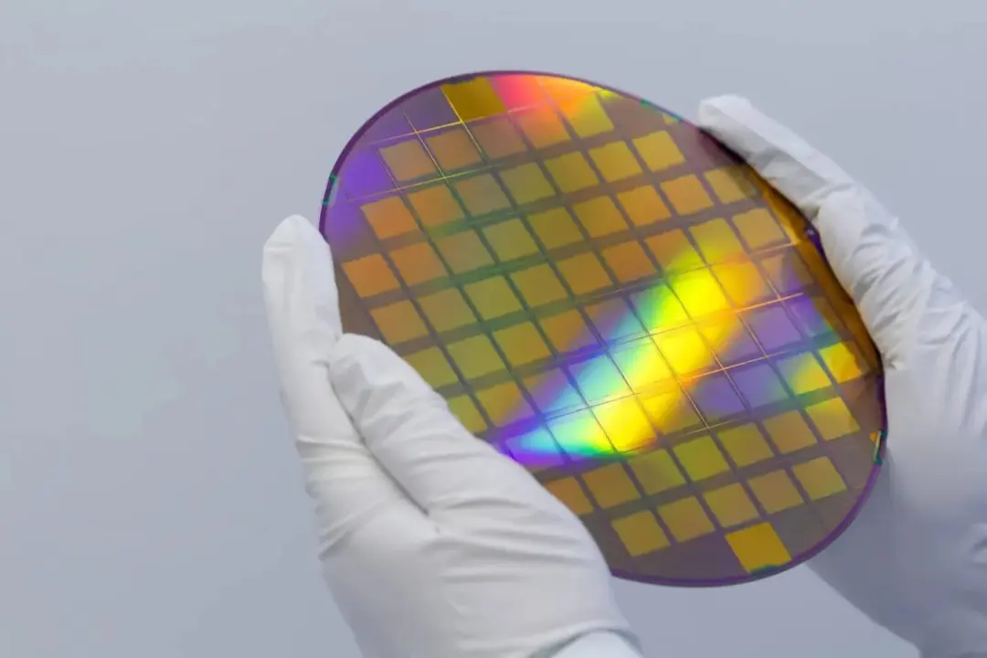
Taiwan government are setting the stage for the next stage of semiconductor manufacturing directly affecting the timing for the advanced chips in high performance computing and robotics. Minister Cheng-Wen Wu recently discussed the new site in Tainan Science and Technology park for the next level TSMC 1nm technology process. This announcement of infrastructure for manufacturing is pointing to the supply chain gearing up for technology beyond mass produced 2nm. For purchasers of next generation technologies it will be interesting to see changes in production that may bring the advanced silicon designs for these technologies to market faster.
Taiwan government and TSMC coordinate resources for 1.4nm manufacturing site in Tainan
The new infrastructure is being developed specifically for TSMC's 1nm or 1.4nm (A14) technology process. Current mass production goals for this technology node is 2028. However, industry rumors indicate this might be pushed to late 2027.
This new infrastructure will be a key site for making the most advanced transistors for the high growth sectors of Robotics and Optical Communications as discussed in the Minister's comments. This discussion points to the growth of semiconductors beyond typical consumer electronics applications.
Advanced technology nodes like this not only require manufacturing capabilities, they also require significant coordination for land and water resources. Minister Wu spoke to the need for coordination of supply chain partners to provide the necessary utilities and land area for the manufacturing facility. In addition to infrastructure, TSMC is also moving ahead with the technology aspect of this transformation with a recent breakthrough in surface engineering technology for transistor manufacturing. This technology partnership with National Yang Ming Chiao Tung University (NYCU) is for optimizing efficiency and performance of transistors for the upcoming technology nodes.
We have been following TSMC's expansion, including earlier stories on land acquisition for two 1.4nm plants with a pilot production in 2027. This earlier story actually supports the current government discussions around ramping up the infrastructure for the 1nm era. Government resource planning and private sector technical breakthroughs together are setting the stage for achieving the 2028 target mass production. This is the confirmed steps that show the industry is gearing up to meet the physical and technical requirements of the sub 2nm process.
The confirmed facts indicate a coordinated effort between Taiwan government and TSMC to create a 1nm manufacturing site in Tainan. This site is for 1.4nm (A14) technology process with a mass production target of 2028. Technical partners are working on surface engineering improvements. The new infrastructure development is ensuring supply chain has the land and water resources in place for the next generation chips.

Does the minister mention specific water consumption metrics for the Tainan facility? The article cites land and water coordination as critical for the 1.4nm process.
No specific numbers are provided in the text. It only states that the government is coordinating resources to ensure sufficient land and water utilities are available for the site.
2028 feels like an eternity for chip tech 🤔
Surface engineering breakthroughs with NYCU are interesting. We need independent power efficiency benchmarks before believing the performance claims for robotics applications.
The article conflates 1nm and 1.4nm. The official node name is A14. Calling it 1nm is marketing shorthand that confuses the actual transistor density metrics.
I just hope the cost of these advanced nodes doesn’t make server racks cost more than my house again.
Industry rumors pushing it to late 2027 should be treated with skepticism. Pilot production in 2027 is already a tight window according to earlier reports.