
TSMC is developing a new packaging technology called CoPoS to address physical size limits in current chip manufacturing. The process replaces traditional silicon interposers with glass substrates sandwiched between ABF layers. This design allows for packages that exceed the standard lithography stencil constraints by more than 9.5 times.
TSMC replaces silicon interposers with glass substrates to overcome physical size limits in chip manufacturing.
NVIDIA plans to use this new packaging architecture for its upcoming Feynman AI chip. The company is expected to be a primary adopter of the CoPoS technology when it becomes available. The shift targets next-generation artificial intelligence silicon that requires larger physical footprints.
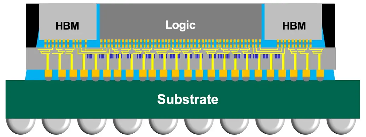
The manufacturing timeline places mass production of CoPoS substrates in 2028. NVIDIA's Feynman chip will likely rely on this process to overcome current hardware limitations. The transition marks a move away from standard interposer designs toward larger glass-based formats.
CoPoS technology directly addresses the size barriers that have constrained previous AI accelerator designs. The new architecture supports significantly larger package dimensions compared to existing solutions. NVIDIA positions the Feynman chip as a key beneficiary of this expanded manufacturing capability.


Discussion
0 comments
Log in to join the thread with a thoughtful take, question, or correction.