
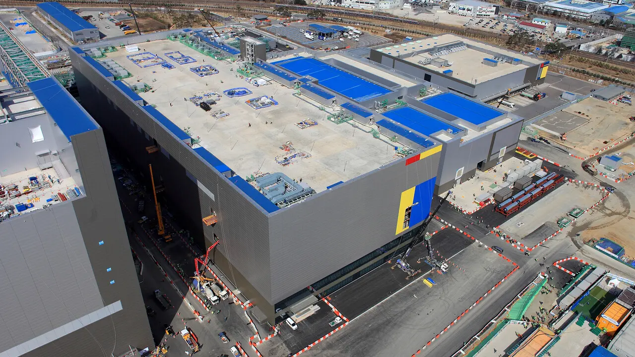
Samsung is expanding its memory chip manufacturing footprint with the construction of P5 Fab 2 in Pyeongtaek, South Korea. The new facility is designed to increase DRAM production capacity, supporting demand from data centers and consumer electronics. The project involves significant investment to expand Samsung's manufacturing capabilities.
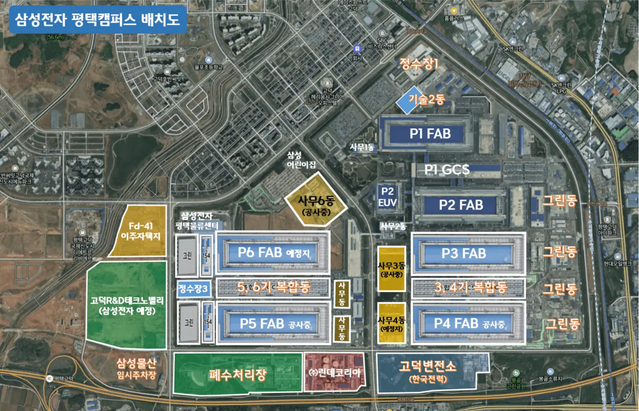
New facility uses 3×3 cleanroom design to boost output
The P5 Fab 2 site will measure 661 meters in length and 194 meters in width. It will operate alongside the existing P5 Fab 1, which is scheduled to begin production in 2028. The facilities will utilize a 3×3 cleanroom design to increase production capacity by at least 50%.
P5 Fab 2 Specifications
- Fab Dimensions: 661 meters length, 194 meters width
- Monthly Wafer Capacity (Per Fab): 300,000 wafers
- Cleanroom Design: 3×3 structure
- Production Capacity Increase: Approximately double current DRAM production
Each fab will have a monthly wafer capacity of 300,000 wafers once fully operational. This combined output aims to nearly double Samsung's current DRAM production capacity, which stands at approximately 650,000 wafers per month. The expanded infrastructure aims to nearly double Samsung's current DRAM production capacity.
Production lines at P5 Fab 1 are expected to start in 2028, followed by P5 Fab 2 in 2029. The entire factory complex is projected to be fully completed in the mid-2030s. Production lines are scheduled to start in 2028 for Fab 1 and 2029 for Fab 2.


Discussion
0 comments
Log in to join the thread with a thoughtful take, question, or correction.