
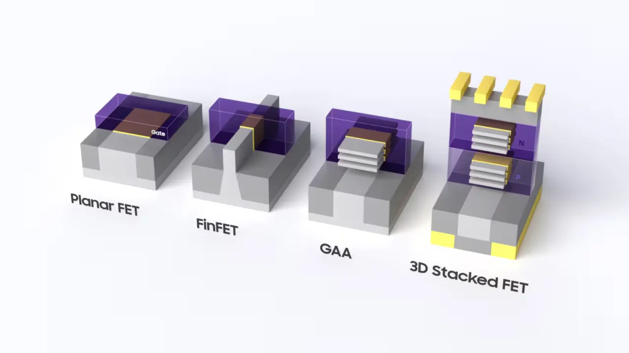
Samsung Electronics demonstrated a new transistor architecture at the 2026 VLSI Symposium, stacking n-type and p-type transistors vertically. The approach extends the Gate-All-Around (GAA) design to achieve higher density without shrinking the transistor footprint.
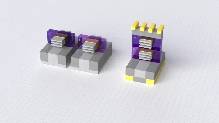
Vertical stacking enables higher transistor density
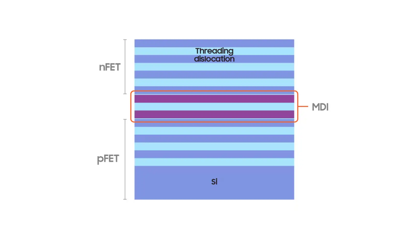
The 3D Stacked FET uses triple stacked nanosheet channels for both n-type and p-type transistors. A key enabler is Middle Dielectric Isolation (MDI), which separates the stacked layers. Samsung also developed a high-quality silicon crystal layer growth process to build the structure.
Specifications
- Gate Pitch: 42 nm
- Channel Configuration: Triple stacked nanosheet channels for both n-type and p-type
- Isolation Layer: Middle Dielectric Isolation (MDI)
The prototype achieves a 42 nm gate pitch, a measure of the distance between adjacent gates. The paper earned a score of 8.29 out of 10 and was selected as Best Paper among over 1,000 submissions at the symposium.
The technology was developed by the Samsung Electronics Semiconductor Research Institute. This technology offers a potential path beyond current GAA transistors, which Samsung already uses in its 3 nm process. No commercial timeline has been disclosed.


Discussion
0 comments
Log in to join the thread with a thoughtful take, question, or correction.