
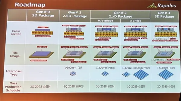
Rapidus has outlined a roadmap for advanced semiconductor packaging that spans several years, targeting the integration of 2nm chips and memory storage. The plan relies on traditional 2D packaging expected in Q3 2028, followed by mass production of 2.5D packaging in Q2 2028. Stronger 2.xD packaging is scheduled for Q1 2029, while 3D packaging using Hybrid-Bonding technology is planned for Q3 2030.
Japanese semiconductor firm Rapidus outlines a phased roadmap for advanced packaging technologies, targeting the integration of 2nm chips and memory storage through traditional 2D to Hybrid-Bonding 3D methods over several years.
Rapidus presents this roadmap as a strategic initiative to strengthen its semiconductor manufacturing capabilities. Advanced packaging efforts target improved chip performance and enhanced memory integration capabilities. The strategy addresses high-performance computing demands by integrating logic and memory via advanced interconnect technologies.
Key technical details include the use of Hybrid-Bonding technology for 3D packaging, which is slated for Q3 2030. The roadmap also emphasizes the transition from traditional 2D to more complex 2.5D and 2.xD configurations. These measures aim to boost chip density and operational efficiency while advancing toward 2nm process nodes.
The timeline suggests a phased rollout of packaging technologies, with each generation building on the previous one. Traditional 2D packaging serves as the foundation before moving to more advanced methods. The integration of memory storage starting from the 2.5D generation highlights a shift toward heterogeneous chip designs.

Discussion
0 comments
Log in to join the thread with a thoughtful take, question, or correction.