
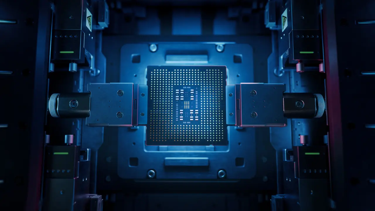
Intel has solved a major packaging bottleneck that was limiting chip size, allowing the company to build packages 24 times larger than the standard industry reticle. This breakthrough matters because it removes the physical ceiling on chip area, enabling manufacturers to pack more compute power into single units without relying on complex multi-chip modules. Buyers of high-end AI accelerators and servers benefit from this shift as it simplifies system design and potentially improves performance density.
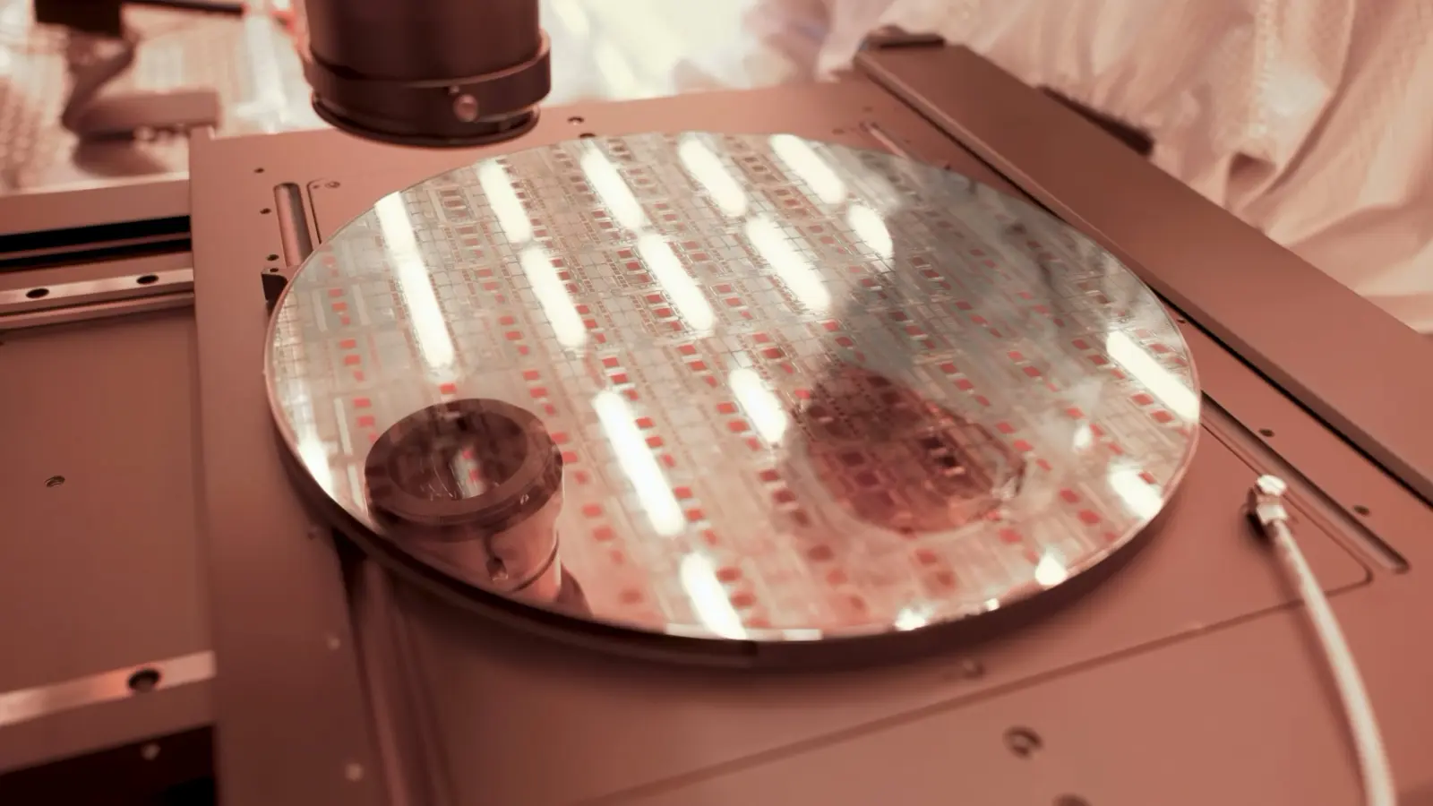
New Hyper-Large Form Factor removes physical ceiling on chip area for AI accelerators
The technology centers on Intel's Hyper-Large Form Factor (HLFF) approach, which utilizes advanced packaging techniques to integrate multiple dies into a single massive substrate. Intel demonstrated this capability at its Rio Rancho facility in New Mexico, which now serves as the United States' leader in advanced packaging. The facility has evolved significantly from its origins as a 6-inch wafer manufacturing hub in the 1980s to handling these complex, ultra-large assemblies today.
The resulting packages measure 240mm by 240mm, a size that exceeds anything the industry has seen except for panel-level packages. Inside these units, EMIB-T bridges with metal layers finer than 2 micrometers connect the components. These bridges support data speeds of 64 Gb/s per channel, which is critical for the high-bandwidth connections required by AI workloads. Intel also validated void-free encapsulation at flow distances of up to 40mm, ensuring structural integrity across the large area.
Power delivery and thermal management require new solutions for chips of this scale. The design embeds silicon capacitors directly beneath the chips to provide up to 1 millifarad of local energy storage per full reticle area. For cooling, Intel proposes a modular, cell-based architecture with independently controlled thermal zones that can handle more than 5 kW of cooling per module. Adding spare communication lanes also raises the bundle yield from approximately 97% to over 99%, making the process more reliable for mass production.

Discussion
0 comments
Log in to join the thread with a thoughtful take, question, or correction.