
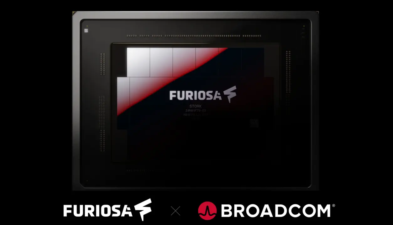
FuriosaAI is moving away from the GPU design playbook for its third-generation AI accelerator. The company claims its new chip, built on a 2nm process with Broadcom, will deliver higher bandwidth and efficiency than the most efficient GPUs available. Sampling is expected by the first half of 2028.
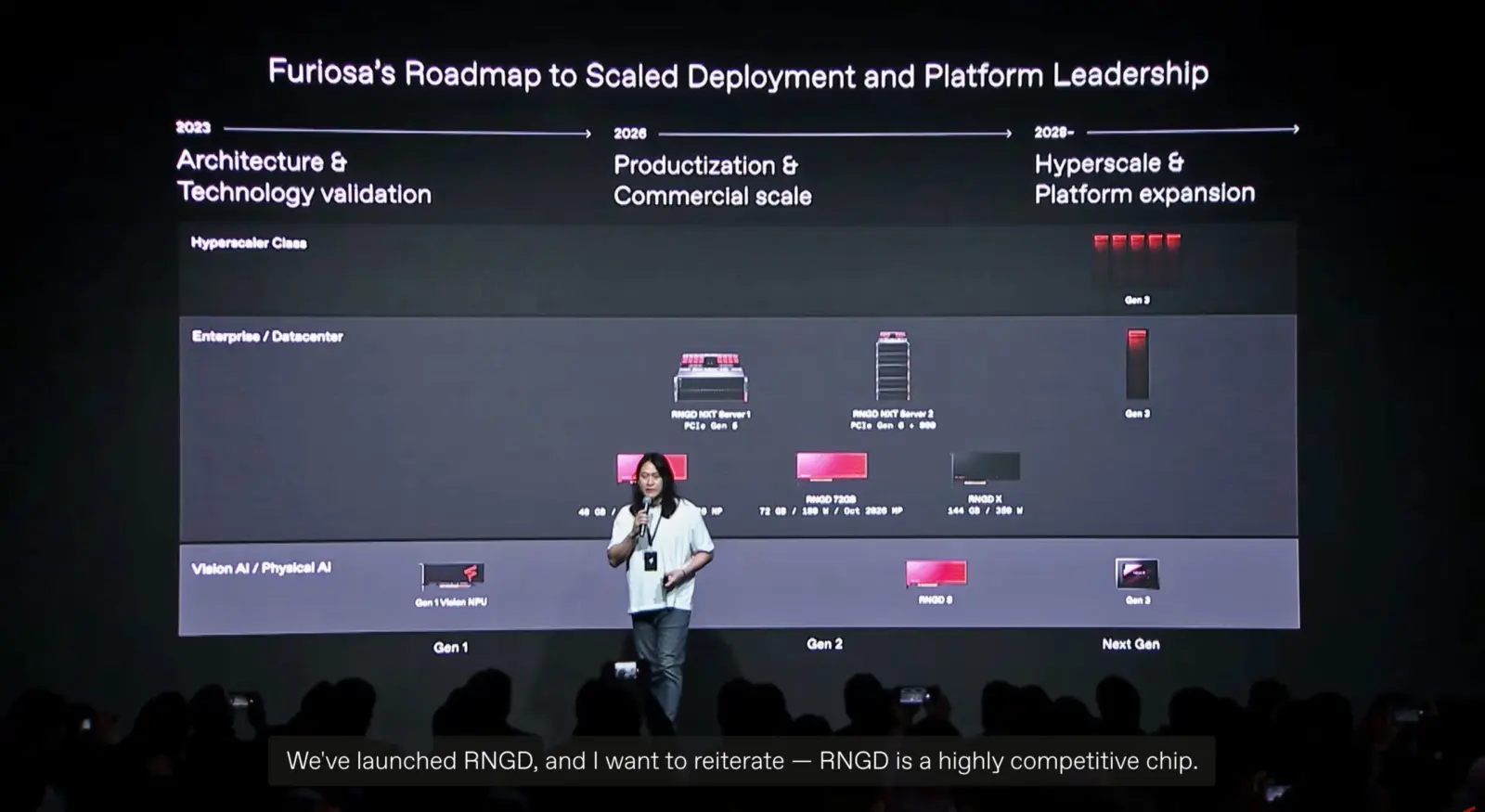
Chiplet design with two 2nm compute dies
The new accelerator, codenamed RNGD, targets AI inference workloads, particularly Agentic AI. FuriosaAI's current RNGD chip is already in mass production and has been adopted by customers including Samsung SDS and LG AI Research.
Specifications
- Process node: 2nm
- Memory: HBM4/E
- Memory sites: 12
- Compute chiplets: 2
- IO controllers: 2
The chip uses a chiplet architecture with two massive 2nm compute chiplets and two IO controllers. It supports HBM4/E memory across 12 memory sites, with a maximum capacity of 432 GB if using 12-Hi 36 GB stacks.
FuriosaAI claims its focus on bandwidth rather than thread management delivers higher efficiency and token throughput than modern GPU designs. The company says the accelerator offers higher performance-per-watt and greater token density than even the most efficient GPUs.
FuriosaAI is partnering with Broadcom for the chip's infrastructure. June Paik, FuriosaAI's CEO, stated that combining Broadcom's infrastructure capabilities with Furiosa's Tensor Contraction Processor architecture allows them to deliver a comprehensive solution for the token factory era.
The third-generation accelerator is expected to begin sampling in the first half of 2028. FuriosaAI has not disclosed pricing. The company's current RNGD chip is in mass production, with Samsung SDS and LG AI Research as customers.
Discussion
0 comments
Log in to join the thread with a thoughtful take, question, or correction.