
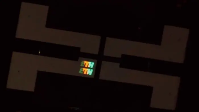
ETH Zurich researchers have demonstrated a new method for manufacturing micro-OLED displays that could eventually enable ultra-compact visual interfaces. This breakthrough matters because it solves a major materials science problem: protecting delicate organic molecules from the harsh chemicals used in standard semiconductor manufacturing. Until now, creating high-resolution organic displays at this scale was not feasible without damaging the light-emitting components.
Tiny organic display proves semiconductor manufacturing can handle delicate materials
The team used a technique called pixel-level photolithography to build the display. Researchers adapted a photolithography technique traditionally used for silicon chips to manufacture organic light-emitting diodes. The result is a tiny, full-color image that proves the technique works for complex visual data. The display itself is only 300 by 430 micrometers in size.
Specifications
- Display Technology: Micro-OLED with pixel-level photolithography
- Image Dimensions: 300×430 micrometers
- Pixel Resolution: 250×350 pixels
- Prototype Size: 1×2.4 millimeters
- Molecular Structure: Core-shell polymer with UV-sensitive outer layer
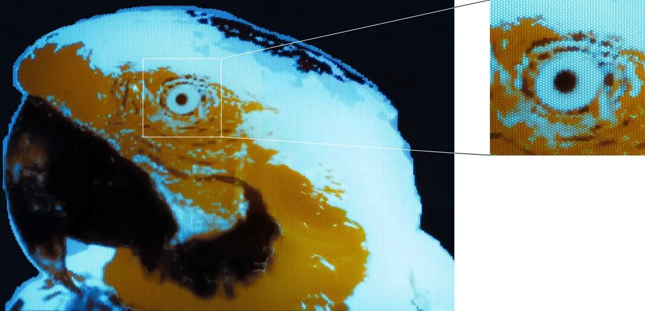
The prototype image contains 250 by 350 pixels, making it the highest-resolution full-color organic structure created via photolithography to date. To achieve this, the researchers designed a special core-shell polymer. The outer shell contains UV-sensitive chemical chains that react during the lithography process, while the inner core protects the light-emitting molecules from chemical damage. This structure allows the organic material to survive the manufacturing steps that would normally destroy it.
The team also built a 1 by 2.4 millimeter prototype of an electrically controlled LOGO. This demonstration shows that the technology can support active electronic control, which is necessary for any practical display application. This research marks a notable advancement in reducing display technology to microscopic dimensions. Previous coverage has examined comparable miniaturization efforts within the broader context of display research.

Discussion
0 comments
Log in to join the thread with a thoughtful take, question, or correction.