

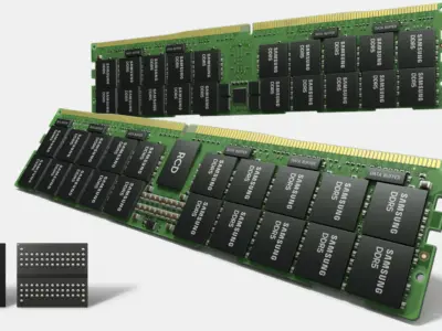
Samsung announced the development of its 10a DRAM on April 24, 2024. Samsung The company plans to target mass production in 2028. This new memory chip utilizes a 4F Square Cell Structure and a Vertical Channel Transistor (VCT) process. Samsung claims this combination marks the first industry adoption of these technologies for DRAM production.
The 10a DRAM features a circuit line width of approximately 9.5 to 9.7 nanometers. Samsung states that the cell density improves by about 30 to 50 percent compared to the 6F Square structure. The company is currently evaluating a replacement for the word line material. Engineers are testing molybdenum to replace titanium nitride, but they face corrosion and process difficulties. Samsung also changed the channel material to indium gallium zinc oxide to reduce leakage current and improve data retention.
Samsung targets global availability for the 10a DRAM in 2028. The company did not announce specific pricing or immediate availability windows for consumers. The announcement focuses on the technical specifications and the long-term production timeline.
Samsung targets 2028 mass production for 10a DRAM with 30-50% density boost
The 10a DRAM represents a significant step in memory technology scaling. Samsung aims to maintain its position in the competitive DRAM market through advanced process nodes. The industry will watch the evaluation phase for the word line material closely as it determines the viability of the 10a node.
Discussion
0 comments
Log in to join the thread with a thoughtful take, question, or correction.