
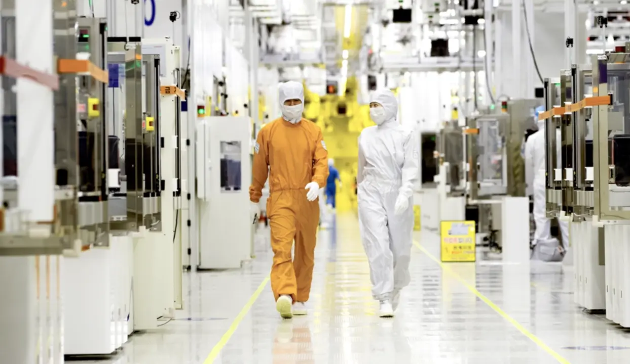
Samsung Electronics joins TSMC in delaying the rollout of ASML's High NA EUV lithography machines, pushing the technology's adoption from the 2-nanometer node to the 1-nanometer (A10) process. This shift matters because it signals that the industry still faces significant hurdles in refining the complex machinery required for next-generation chip manufacturing. Buyers and investors should note that the timeline for these advanced nodes has slipped, potentially affecting the pace of performance gains in future processors.
Samsung shifts High NA EUV adoption from 2nm to 1nm node
The core hardware in question is the High NA EUV machine, a 165-ton tool built by ASML that uses extreme ultraviolet light at a wavelength of 13.5 nanometers. Samsung's VP of Technology, ChangMin Park, confirmed during a conference in Korea that the company will deploy these machines for technologies starting at the 1-nanometer manufacturing node. This represents a strategic pivot from Samsung's earlier plans to utilize the equipment for volume production of 2-nanometer and 1.4-nanometer process nodes.
Key Specifications
- Numerical Aperture: 0.55NA
- Wavelength: 13.5 nanometers
- Tool Weight: 165-ton
- Target Node: 1-nanometer (A10)
- Mass Production: 2030
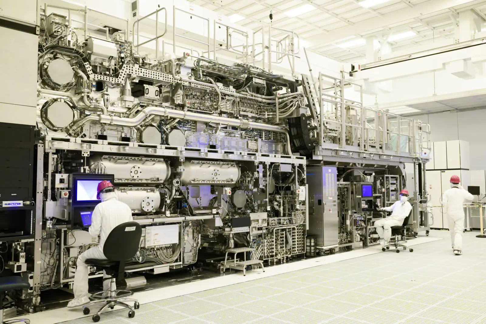
High NA EUV technology features a numerical aperture of 0.55NA, which allows for the printing of smaller circuits compared to standard EUV systems. This higher precision helps reduce the costs and defects associated with multi-patterning techniques used in advanced chip fabrication. The 165-ton tool is designed to handle the increased complexity of these smaller geometries, though the technology remains in a developmental phase for mass adoption.
Samsung previously expected to use the High NA EUV machines for the 2nm and 1.4nm nodes, but the delay implies a need for further refinement of the equipment or processes. Mass production of chips using this 1-nanometer technology is now expected as early as 2030. We touched on ASML High-NA EUV EXE in our earlier Asml coverage when tracking throughput capabilities for AI chips, but Samsung's current focus remains on the 1nm node.
The confirmed facts center on Samsung's decision to align with TSMC in stalling the High NA EUV rollout to the 1-nanometer node. The equipment remains a 165-ton system with 0.55NA capability, and mass production is targeted for 2030. This delay highlights the ongoing technical challenges in scaling semiconductor manufacturing to the 1-nanometer era.

Discussion
0 comments
Log in to join the thread with a thoughtful take, question, or correction.