

Intel has achieved a breakthrough in ultra-large-scale chip packaging, manufacturing units that exceed 12 times the size of a standard photolithography mask. This advancement matters because it allows the company to integrate more silicon into a single package, a critical step for high-performance computing and AI infrastructure. Server and data center buyers should take note, as larger packages can reduce interconnect complexity and improve system efficiency.
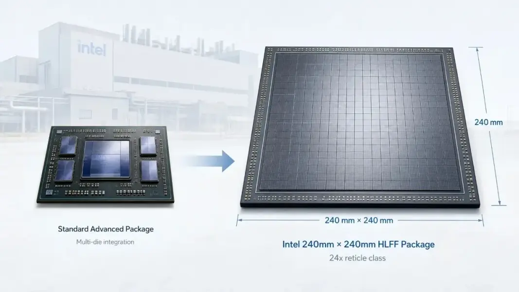
New 240mm package enables more silicon in single unit
The current package size measures 240mm by 240mm, which represents a 24x mask ratio. This figure stands at eight times the current industry standard for similar packaging technologies. Intel developed this capability at its facility in Rio Rancho, New Mexico, using advanced embedding technologies.
- Current Package Size: 240mm x 240mm
- Current Mask Ratio: 24x
- Current Industry Standard Ratio: 8x
- Planned Ratio (2028): 12x
- EMIB Underfill Flow Distance: 43mm
The company utilizes EMIB, or Embedded Multi-die Interconnect Bridge, to link multiple chiplets within the package. Standard packaging typically limits the underfill material flow distance to 22mm, but Intel's new process reaches 43mm. This longer flow distance requires optimized underfill material formulation and a multi-point dispensing strategy to eliminate bubbles during the curing process.
Intel plans to expand its packaging capabilities to a ratio of 12x or higher by 2028. Panel-level packaging could potentially increase this ratio to over 50x in the future. We looked at TSMC CoWoS Bottleneck Pushes Intel EMIB earlier while tracking these packaging advancements.
Intel has confirmed the physical dimensions and technical methods behind its latest packaging breakthrough. The company is actively optimizing its manufacturing processes in Rio Rancho to support larger chip integration.

Discussion
0 comments
Log in to join the thread with a thoughtful take, question, or correction.