
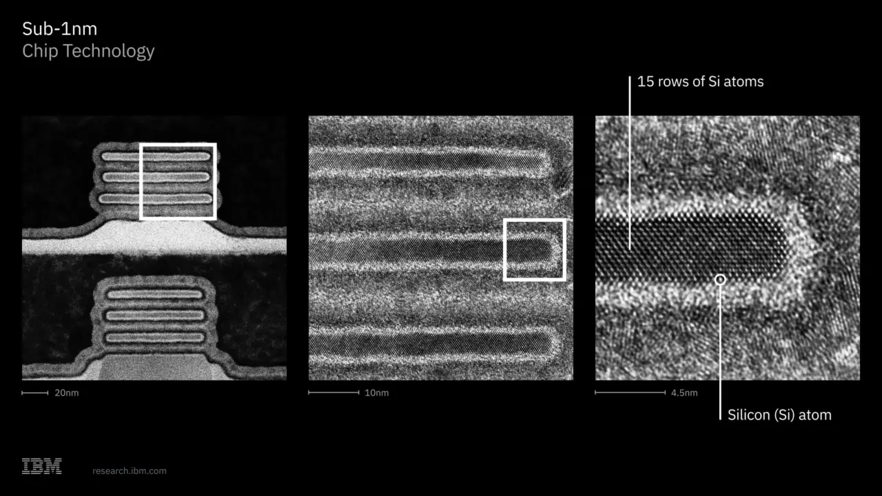
IBM has introduced a new semiconductor manufacturing process that pushes chip fabrication beyond the one-nanometer threshold. This development matters because it establishes a clear path for future hardware to deliver significantly higher computational power while consuming less energy. Buyers and engineers can expect this technology to enable more compact and efficient devices in the coming years.
New architecture stacks transistors vertically for massive density gains
The company calls this architecture Nanostack, a design that moves away from traditional flat layouts. Instead of placing components side by side, the structure vertically stacks and staggers transistors to create a three-dimensional integration. This approach allows for a much denser packing of electronic components within the same physical footprint.
Key Specifications
- Process Node: 0.7 nanometer
- Transistor Density: 100 billion (fingernail-sized area)
- Performance Improvement: 50% vs 2nm
- Power Efficiency: 70% higher vs 2nm
- AI Chip Speed: 9,000 TOPS
IBM claims the 0.7-nanometer technology can pack 100 billion transistors into an area the size of a fingernail. This density is nearly double that of the firm's previous 2-nanometer chips announced in 2021. The firm validated the design through experimental ultra-thin dielectric bonding in CMOS integration, a method that creates robust multilayered structures.
Performance metrics show a 50 percent improvement over 2-nanometer chips, with power efficiency rising by 70 percent. For artificial intelligence workloads, an AI chip built on this process could achieve 9,000 trillion operations per second. This speed boost reduces model training time from three months down to just a couple of weeks.
IBM has not yet announced specific consumer products or a release date for this manufacturing node. The focus remains on the technical validation of the Nanostack architecture and its potential to advance semiconductor capabilities. This announcement confirms the viability of sub-1nm chipmaking as a next step in hardware evolution.


Discussion
0 comments
Log in to join the thread with a thoughtful take, question, or correction.