
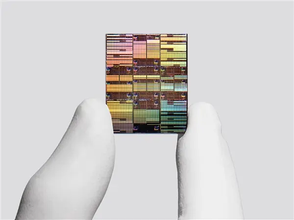
IBM has demonstrated a semiconductor breakthrough that could redefine how the industry approaches physical limits in chip manufacturing. The company unveiled a prototype chip built on a 0.7nm process node, which translates to 7 Angstroms. This development matters because it proves that transistor scaling can continue well beyond the traditional 1nm barrier. Buyers and engineers now have a concrete example of how vertical stacking can overcome the density constraints of flat silicon designs.
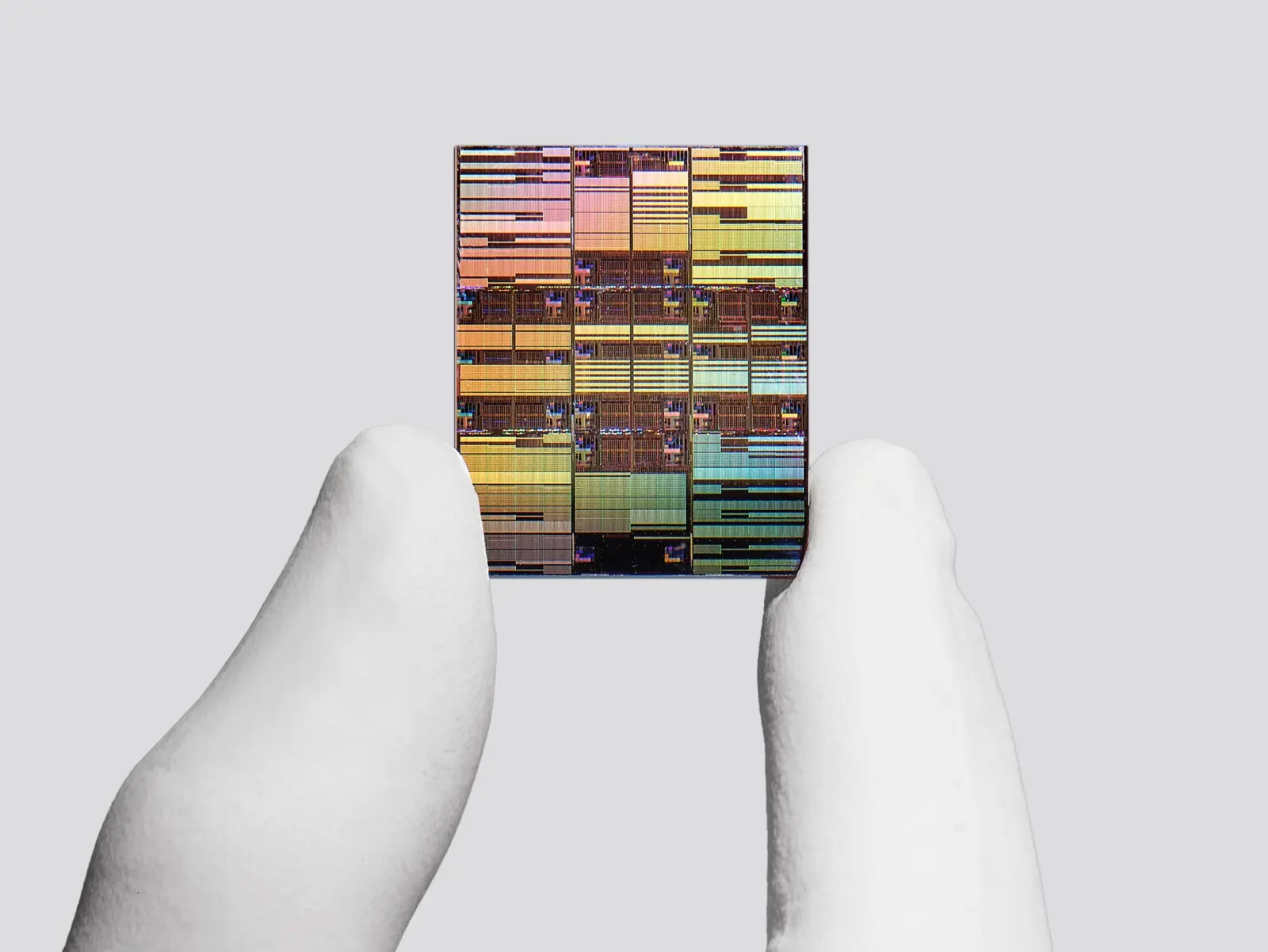
IBM demonstrates 0.7nm chip with 100 billion transistors and 3D Nanostack architecture
The prototype integrates 100 billion transistors into a physical area roughly the size of a human nail. IBM achieved this density through a proprietary architecture called 3D Nanostack. This design replaces the standard planar layout with a vertical arrangement of nanosheets. The structure allows transistors to stack on top of each other rather than spreading out horizontally.
Specifications
- Process Node: 0.7nm (7 Angstroms)
- Transistor Count: 100 billion
- Performance Improvement: Up to 50% vs 2nm
- Energy Efficiency Improvement: Up to 70% vs 2nm
- Architecture: 3D Nanostack
Performance metrics for the 0.7nm chip show a 50 percent improvement over IBM's previous 2nm chip released in 2021. Energy efficiency gains reach 70 percent compared to that same baseline. The 3D Nanostack architecture reduces the area required for static random-access memory by 40 percent. These figures come directly from IBM's technical specifications for the prototype.
IBM plans to introduce high-numerical-aperture extreme ultraviolet lithography machines to support future manufacturing steps. The company is also establishing a new pure-play quantum wafer foundry subsidiary named Anderon. These infrastructure moves aim to support the complex production requirements of advanced nodes. The prototype currently exists as a demonstration of technical feasibility rather than a commercial product.
Mass production of the 0.7nm chip is not imminent. IBM estimates that bringing this technology to market will take at least five years. The company has confirmed the technical viability of the process but has not set a specific launch date. The announcement serves as a roadmap for the next phase of semiconductor development.

Discussion
0 comments
Log in to join the thread with a thoughtful take, question, or correction.