
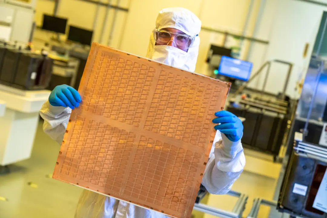
TSMC is shifting its advanced packaging strategy toward square and rectangular panels to replace the traditional circular wafers used in CoWoS technology. This move directly addresses the geometric waste that has long limited manufacturing efficiency for high-performance AI and GPU chips. Buyers and system integrators will see improved supply chain stability as TSMC aims to boost material utilization rates significantly above current industry standards. The transition represents a fundamental change in how semiconductor manufacturers handle substrate geometry and cost structures.
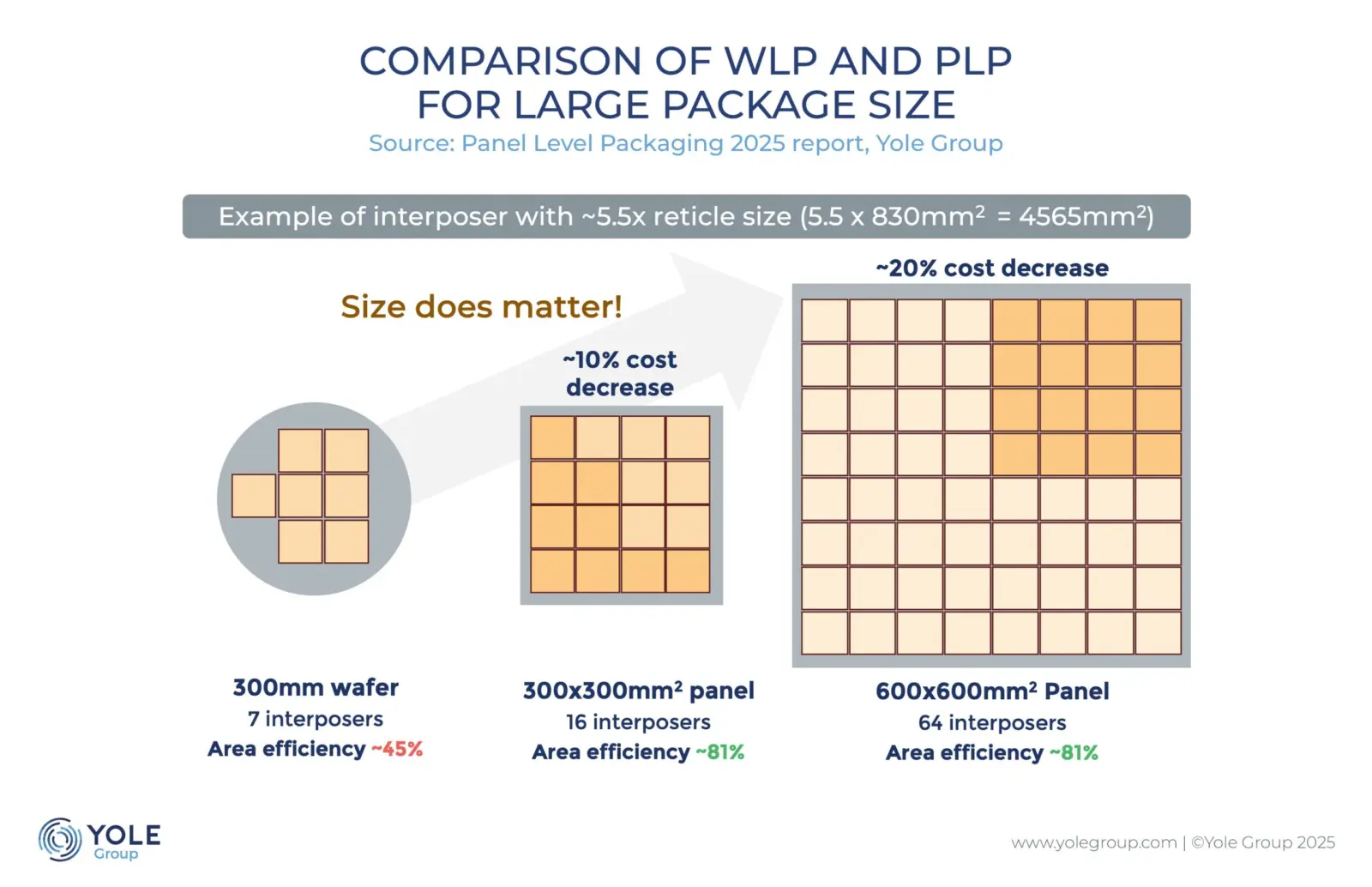
Square panels replace circular wafers to improve yield
The new CoPoS platform relies on glass core substrates to achieve its performance goals. These substrates feature a three-layer design where a glass core sits between two ABF layers. TSMC is collaborating with partners Ibiden and Innolux to develop these specific 3-layer structures. This technical approach allows the company to surpass the physical limits of existing CoWoS packaging methods.
Specifications
- Wafer Size: 750x620mm, 310x310mm, 515x510mm
- Wafer Utilization: Past 90%
- Cost Reduction: 30%
- Glass Substrate Design: 3-layer (glass core sandwiched between two ABF layers)
CoPoS panels can measure up to 750x620mm, with additional sizes of 310x310mm and 515x510mm available for different production needs. This square format transforms the circle into a square, which significantly increases the material utilization rate from less than 70% to more than 90%. The technology delivers higher volumes at 20-30% lower costs per unit area compared to CoWoS. These metrics highlight the economic advantage of moving away from circular wafer constraints.
Trial production for CoPoS is scheduled to begin in 2027, with mass production expected in the second half of 2028. TSMC Arizona is projected to play a major role in this production phase between 2029 and 2030. The timeline for CoPoS specifically using glass core substrates is set for 2030 or later. This phased rollout allows TSMC to refine yield rates before full-scale deployment across its global manufacturing network.

Discussion
0 comments
Log in to join the thread with a thoughtful take, question, or correction.