
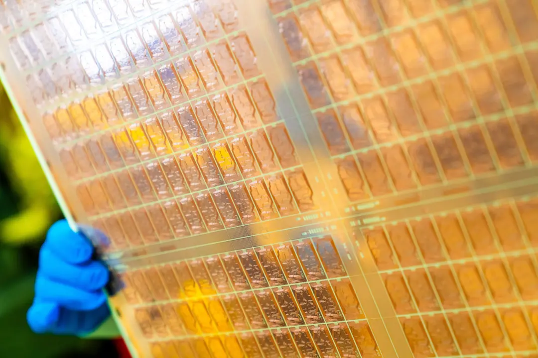
TSMC has clarified that its upcoming panel-level packaging technology will not replace the company's existing wafer-based CoWoS platform for high-end artificial intelligence processors. Senior Vice President Kevin Zhang stated that panel manufacturing lacks the interconnection density required for the most advanced chip designs. This distinction ensures that wafer-level processes remain critical for large-scale AI accelerators despite industry shifts toward larger packaging formats.
Wafer-level packaging retains density advantage while panel tech scales to larger dimensions by 2030
The company is currently developing CoPoS, a new panel-based packaging solution designed to handle significantly larger physical dimensions than current standards allow. TSMC plans to complete its first CoPoS pilot line in June of this year. The technology aims to scale from initial 310mm by 310mm panels up to maximum sizes of 750mm by 620mm for future production runs.
- Panel Packaging Dimensions: 310mm x 310mm initial, scaling to 515mm x 510mm or 750mm x 620mm
- Wafer-Level Substrate Dimensions: Current: 120mm x 150mm; Next-gen CoWoS: 150mm x 250mm
- CoWoS Scaling Capacity: Up to 58 large reticle-sized dies in one package
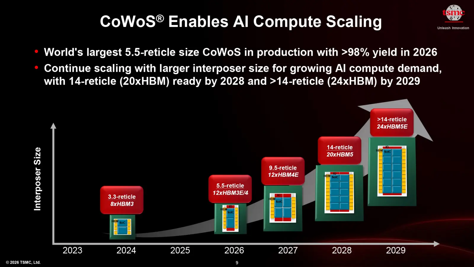
Current wafer-level substrates used in CoWoS measure 120mm by 150mm, but next-generation versions will expand to 150mm by 250mm. This scaling allows engineers to integrate up to 58 large reticle-sized dies into a single package. The geometric complexity of panel-based processes cannot match the capabilities of wafer-level manufacturing at this stage.
Zhang emphasized that moving from wafer to panel technology requires rapid improvements in process control to eventually offer a superior next-generation solution. High-volume manufacturing for CoPoS products is not expected until 2029 or 2030 due to these technical hurdles. The industry must advance panel processes quickly to compete with the established density advantages of wafer-level tech.
CoWoS and CoPoS will function as complementary technologies rather than direct replacements for each other in the near term. Wafer-level packaging retains its position where high interconnection density is paramount, while panel packaging addresses the need for larger physical footprints. This dual-track approach supports the growing demand for complex AI hardware architectures.
Discussion
0 comments
Log in to join the thread with a thoughtful take, question, or correction.