
Samsung and SK hynix are pursuing distinct manufacturing strategies for next-generation DRAM chips to address the tight market conditions driven by AI data center demand.
Samsung explores Gate-All-Around FET technology for next-generation memory production
The competition aims to establish their respective approaches as the standard model for the next-generation DRAM market.
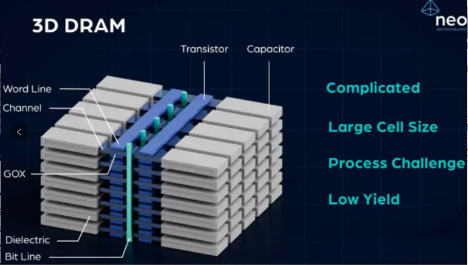
Samsung is considering the application of Gate-All-Around FET (GAAFET) technology for its next-generation DRAM production.
This approach involves placing control circuits under the memory array, similar to the circuit placement used in NAND manufacturing.
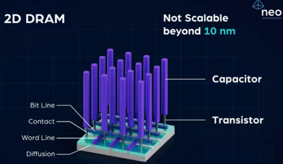
SK hynix is experimenting with a 4F² approach that features the vertical stacking of transistors.
In this method, the gate retraction occurs on the side of the vertically stacked transistors.
SK hynix experiments with vertical transistor stacking using a 4F2 approach
Demand for high-bandwidth memory, DRAM, and other chips has become tight due to increased computing needs for AI data centers.
Samsung and SK hynix are competing to define the industry standard for these critical memory components.
Samsung has not confirmed whether it will proceed with GAAFET production for DRAM.
SK hynix is currently in the experimental phase with its 4F² approach.
Discussion
0 comments
Log in to join the thread with a thoughtful take, question, or correction.