
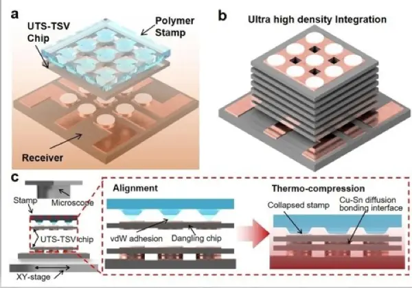
Researchers at Pohang University of Science and Technology (POSTECH) have developed a method to stack ultra-thin semiconductor chips with significantly higher density than current standards. This advancement matters because it offers a pathway to increase memory capacity without expanding the physical footprint of AI accelerators and high-performance processors. The breakthrough addresses critical bottlenecks in chip manufacturing that have limited the density of existing High Bandwidth Memory (HBM).

Research milestone offers post-Moore path for AI accelerators
The team integrated transfer printing and real-time bonding into a single stable process to handle silicon chips that are approximately 14 micrometers thick. This approach allows for the stacking of more than ten layers while keeping the total thickness minimal. By combining these steps, the researchers avoided the alignment errors and warping that typically plague ultra-thin chip assembly.
Specifications
- Stacking Density: Approximately 4x that of existing HBM
- Chip Thickness: Approximately 14 micrometers
- Stacking Layers: 10+ layers
- Processing Temperature: Below 180 degrees Celsius
- Alignment Error: Almost zero offset
The processing conditions remain gentle, operating at temperatures below 180 degrees Celsius and pressures under 20 kilopascals. These low-stress parameters help suppress chip warping and result in almost zero offset between layers. The precision of this alignment is crucial for maintaining electrical connectivity across the dense stack.
The resulting integration density reaches approximately four times that of existing HBM technology. This density increase means manufacturers can pack more memory into the same area, which is vital for data-intensive workloads. The research findings have been published in the journal Results in Engineering.
The specific commercial timeline for this technology remains unconfirmed as the source focuses on the academic publication of the results. Buyers and industry observers should note that this is a research milestone rather than an immediate product release. The technology provides a viable path for post-Moore era chip development.
Discussion
0 comments
Log in to join the thread with a thoughtful take, question, or correction.