
Intel plans to launch a 14A2 process node, a modified version of its 14A technology, to compete directly with TSMC and Samsung in the 1.4nm-class segment. This update matters because it signals Intel's intent to close the manufacturing gap with its primary rivals by adopting a more aggressive power delivery architecture. Buyers tracking long-term CPU and GPU silicon roadmaps should watch how this dual-side power approach scales in production.
Intel plans dual-side power delivery and 21nm pitch for 14A2 node
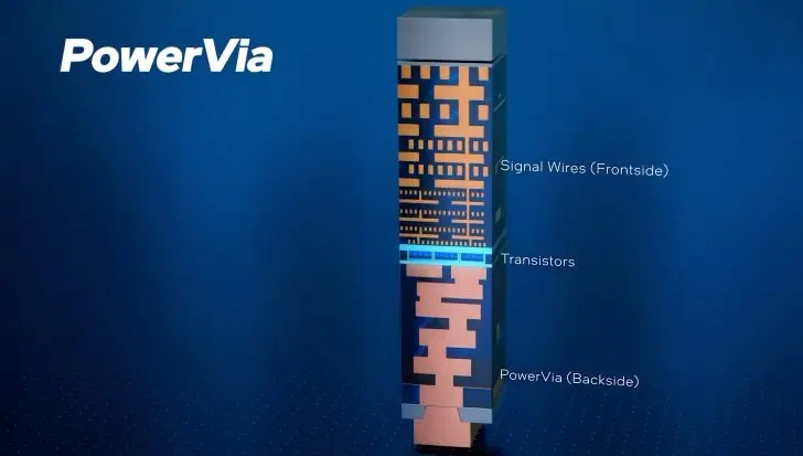
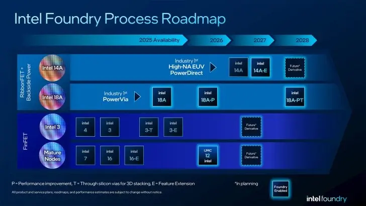
The 14A2 node, also referred to as 14A Gen2, introduces a dual-side power delivery system that combines back-side power with retained front-side power. Intel developed this configuration to address the technical challenges posed by shrinking interconnect dimensions in more advanced manufacturing nodes. The company employs a back-side power technology called PowerDirect to support this hybrid architecture, aiming for greater stability as transistor density increases.
Specifications
- Process Node: 14A2 (14A Gen2)
- Power Delivery Architecture: Dual-side power delivery (retaining partial front-side power while adding back-side power)
- Back-side Power Technology: PowerDirect
- Minimum Metal Interconnect Layer (M0) Pitch: Approximately 21nm (reduced from ~28nm in 14A)
- PDK Release: 0.9 version for external customers in October 2026
A key technical change in the 14A2 process is the reduction of the minimum metal interconnect layer pitch from approximately 28nm in the 14A node to about 21nm. Intel states that this tighter pitch aims to increase transistor density while improving the economic efficiency of High-NA EUV lithography equipment. These specifications define the physical limits of the node and its potential performance gains over previous generations.
Intel plans to release the 14A 0.9 process design kit to external customers in October 2026, laying the groundwork for third-party adoption. The company targets risk production for the 14A2 node in 2028, with mass production scheduled to follow in 2029. Intel also aims to secure orders from large fabless chip design enterprises within 18 months of the PDK release, though this remains a goal rather than a confirmed contract.
We looked at Intel Restarts 13th and 14th Gen in our earlier Intel coverage to track ongoing manufacturing adjustments at the company. The 14A2 roadmap aligns with competitor timelines, as TSMC and Samsung also target 2028 to 2029 for their respective 1.4nm-class nodes. This parallel timing highlights the intense competition in the next generation of semiconductor manufacturing.
Intel confirms the 14A2 process will utilize dual-side power delivery and a 21nm interconnect pitch, with mass production set for 2029. The company continues to refine its manufacturing capabilities to meet the demands of advanced logic nodes. External customers can expect access to design tools in 2026, with production readiness following in the subsequent years.
Discussion
0 comments
Log in to join the thread with a thoughtful take, question, or correction.