
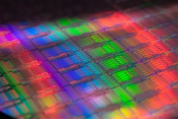
Intel’s 14A process has hit a defect density of 0.5 and a 40% yield, according to a Morgan Stanley report. The milestone positions Intel to compete for 1.4nm node customers against TSMC.
Defect density expected to drop further
The 14A process is Intel’s next-generation manufacturing node. It is key to the company’s foundry ambitions and its ability to win external chip orders.
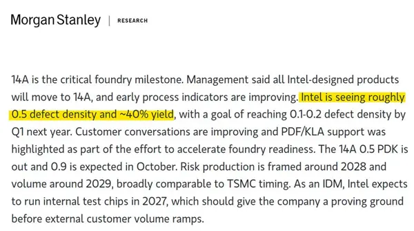
Defect density is expected to drop to between 0.1 and 0.2 by the first quarter of 2026. Risk production is scheduled for 2028, with mass production planned for 2029.
Internal chip testing could begin as early as 2027. The timeline gives Intel several years to refine the process before commercial shipments.
Mass production is set for 2029, according to the report. When we covered the last 14a process update, several of the same balance and stability themes came up.



Discussion
0 comments
Log in to join the thread with a thoughtful take, question, or correction.