
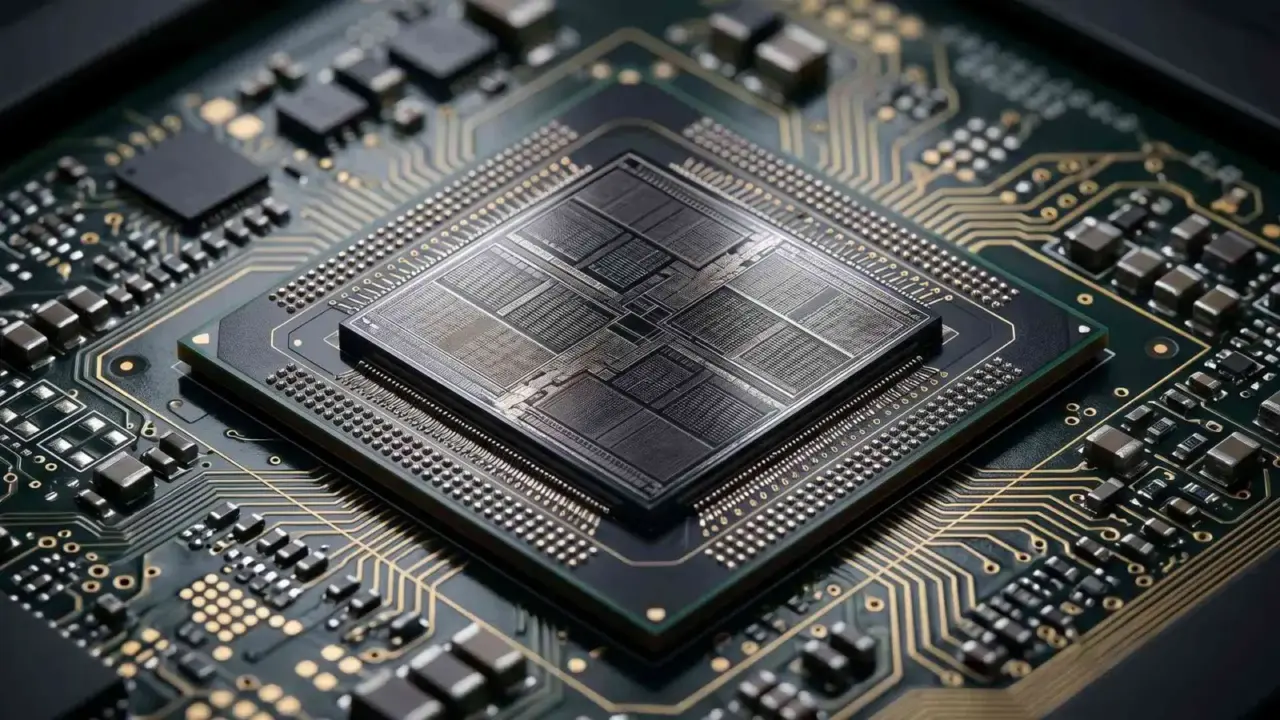
Samsung and SK hynix are developing competing manufacturing techniques for next-generation DRAM chips. The industry is currently facing tight supply conditions driven by the rapid expansion of AI data centers. This surge in demand has strained the markets for high-bandwidth memory and standard DRAM components.
Samsung explores gate-all-around FET technology for upcoming memory products
Samsung is exploring the use of gate-all-around FET technology for its upcoming memory products. The company plans to place the circuitry that manages read and write operations underneath the memory array. This structural approach borrows directly from manufacturing methods used in NAND flash storage.

SK hynix is pursuing a different path with its 4F squared manufacturing approach. This method involves stacking transistors vertically and wrapping the gate material around the transistor pillars. Both vendors are reportedly racing to have their respective techniques recognized as the new industry standard.
The competition between these two major memory manufacturers highlights the intense pressure on the supply chain. AI-driven buildouts have created a bottleneck that affects multiple segments of the semiconductor market. Establishing a new standard will likely determine which company leads the next era of memory technology.

Industry insiders suggest that Samsung and SK hynix are eager to set the standard first. Neither company has officially confirmed the specific timeline for these new manufacturing processes. The race to define the next generation of DRAM architecture remains ongoing.


Discussion
0 comments
Log in to join the thread with a thoughtful take, question, or correction.