
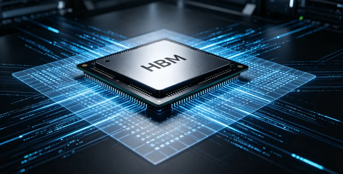
Kepler Computing has stepped out of a seven-year stealth period to reveal a new memory architecture that could reshape how high-density memory is manufactured. The startup claims its approach removes the need for extreme ultraviolet lithography, a critical and expensive tool that currently limits global supply of high-bandwidth memory. This shift matters because it offers a path to increase memory density without requiring the construction of new, costly fabrication plants. Buyers and system integrators should watch this development closely as it targets the severe bottlenecks currently constraining AI and high-performance computing hardware.
Startup aims to increase memory density without new fabrication plants
The company was co-founded by former Intel executive Sasi Manipatruni and currently operates with CEO Debo Olaosebikan leading the organization. Kepler Computing focuses on developing advanced memory solutions, specifically targeting high-bandwidth memory and static random-access memory. Their technology relies on a combination of 3D stacking techniques and proprietary ferroelectric materials to achieve higher performance and density. This architectural choice allows them to bypass the traditional constraints associated with standard semiconductor manufacturing processes.
- Technology: 3D stacking and proprietary ferroelectric materials
- Manufacturing Constraint: Does not rely on EUV lithography
- Target Product: HBM and SRAM
- Production Status: Validated on approx. 2000 wafers
- Manufacturing Partner: GlobalFoundries
The core technology utilizes 3D stacking to layer memory components, which significantly increases density per unit area. The company uses proprietary ferroelectric materials that do not require extreme ultraviolet lithography for production. This manufacturing constraint removal means existing production lines can be modified rather than replaced to increase output. The technology has already undergone validation on approximately 2000 wafers, demonstrating that the process is viable at a significant scale.
Kepler Computing has partnered with GlobalFoundries to handle the manufacturing aspects of this new technology. The company plans to ship its first high-bandwidth memory samples in late 2024 to early customers. Production expansion is scheduled to begin in Singapore in 2025, with domestic production in the United States targeted for 2028. These timelines indicate a phased rollout aimed at gradually increasing supply to meet market demand.
GlobalFoundries executive Ed Kaste has noted that iron is a difficult contaminant to manage in production facilities. The ferroelectric materials used by Kepler contain iron, which requires specialized equipment or complete encapsulation to handle safely. This technical challenge remains a key consideration for the feasibility of mass production. The company must address these contamination risks to ensure long-term manufacturing stability.
Kepler Computing has secured backing from major industry players, including Intel Capital, AMD Ventures, and GlobalFoundries. This financial support underscores the industry interest in their approach to solving memory supply constraints. The company aims to alleviate global high-bandwidth memory shortages by modifying existing infrastructure. Their strategy focuses on increasing supply through efficiency gains rather than capital-intensive new builds.
Discussion
0 comments
Log in to join the thread with a thoughtful take, question, or correction.