
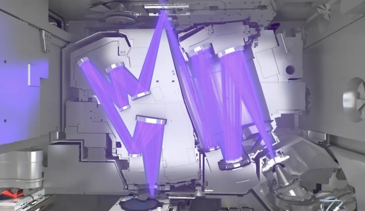
Samsung is shifting its semiconductor strategy by integrating quantum computing algorithms into chip manufacturing. This move targets the lithography and etching stages, which currently consume significant time and resources during fabrication. Reducing these bottlenecks allows manufacturers to increase chip density and improve overall production yields. Buyers in the tech sector should watch this development as it signals a new approach to maintaining competitive edge in advanced node production.
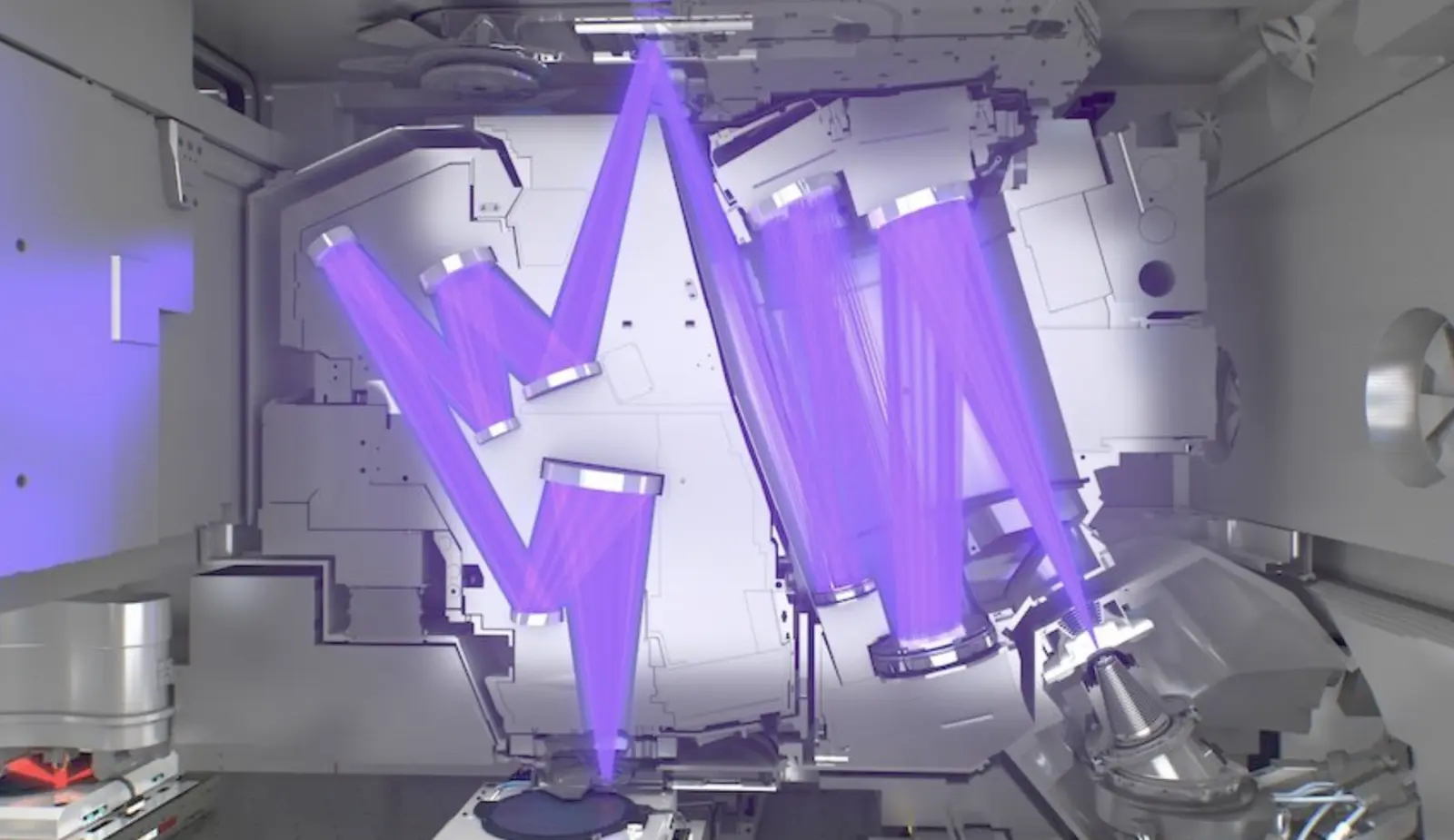
The tech giant aims to reduce fabrication time and improve chip yields
Samsung SDS, the technology services arm of the Samsung Group, is leading the development of these simulation algorithms. The company is combining artificial intelligence with quantum computing to model light behavior during the lithography process. This technical approach aims to replace or augment traditional simulation methods that are often slow and computationally expensive. The project represents a direct effort to modernize the foundational software tools used in semiconductor design.
The core objective of this initiative is to lower the time and cost associated with chip fabrication. By optimizing the simulation of light patterns, the algorithms help engineers achieve higher precision in pattern transfer. This precision is critical for maintaining manufacturing yield as transistors shrink to smaller nodes. The firm has already secured the necessary algorithms and is moving toward a verification phase.
Samsung plans to verify these algorithms through a proof of concept scheduled for next year. If the simulation software proves viable, the firm is expected to share the technology with Samsung Electronics. This subsidiary is the company's flagship unit responsible for actual chip production. The development positions Samsung to compete more effectively with TSMC, which already utilizes AI in its fabrication nodes.


Discussion
0 comments
Log in to join the thread with a thoughtful take, question, or correction.