
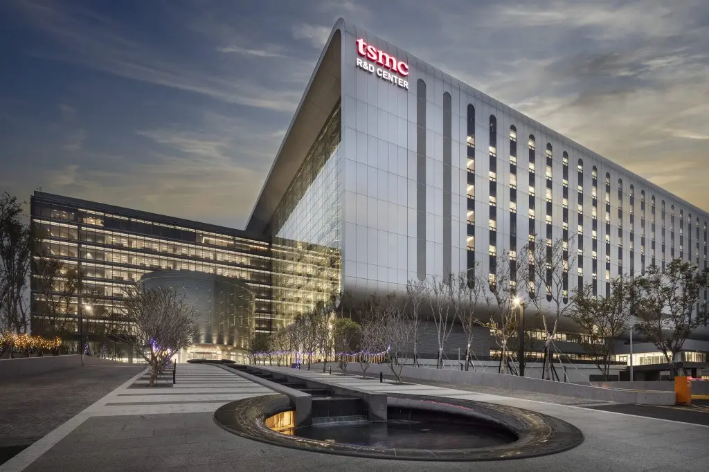
TSMC has confirmed its CoPoS (Chip-on-Panel-on-Substrate) pilot line is already running, with mass production expected within two to three years. Chairman C.C. Wei stated at the early June shareholders' meeting that the panel-level packaging line is operational. This move targets advanced packaging for future chips.
Dual sourcing strategy for panel-level packaging
CoPoS uses 310x310mm panels, a shift from traditional wafer-level packaging. TSMC is evaluating equipment from both global and Taiwanese suppliers. Potential vendors include DISCO, Lintec, Nitto, Yamada, Tazmo, Gudeng, Mirle, Applied Materials, Tokyo Electron, SCREEN, Scientech, GPTC, Utechzone, VisEra, GPM, KLA, and Camtek.
The company plans to build a small production line at VisEra in 2026, start trial production in 2027, and reach mass production between 2028 and 2029. This timeline aligns with the expected ramp-up of CoPoS technology.
Samsung Electronics is also developing panel-level packaging, shifting from 600x600mm to 415x510mm panels to reduce warpage. South Korean equipment makers GigaVis, Semes, and Hanwha Semiconductor are entering the PLP market. According to a source, GigaVis may supply PLP equipment to Samsung, though this is unconfirmed.
TSMC's CoPoS pilot line evaluation triggers competition among domestic and foreign equipment suppliers. The company is pursuing a dual sourcing strategy to secure the best tools for panel-level packaging.
Discussion
0 comments
Log in to join the thread with a thoughtful take, question, or correction.