

TSMC has announced its A16 process node, which the company describes as a 1.6nm technology. The A16 node represents a significant step in the semiconductor industry's push for higher efficiency and performance. The announcement highlights specific technical improvements over the previous N2P node, focusing on speed, power consumption, and density.

The A16 node promises an 8 to 10 percent speed increase compared to the N2P node when measured at the same core area. In terms of power efficiency, the technology delivers a 15 to 20 percent reduction in power consumption at the same speed. Additionally, A16 provides a maximum logic density gain of 1.10 times relative to N2P. A key feature of this architecture is the inclusion of Super Power Rail technology. The Super Power Rail (SPR) technology is designed to enhance power distribution efficiency across the chip.
New process node delivers significant speed and power improvements over previous generation technology
Mass production of chips using the A16 process is scheduled to begin in the fourth quarter of 2026. Despite the start of manufacturing, actual product launches are expected to occur between 2027 and 2028. The interval between Q4 2026 manufacturing start and 2027-2028 product launch aligns with standard timelines for integrating new process nodes into commercial devices.
Spec comparison
| Spec | A16 |
|---|---|
| Process Node | 1.6nm (A16) |
| Performance Gain vs 2nm | 8~10% speed increase |
| Power Consumption Reduction vs 2nm | 15~20% reduction |
| Logic Density Gain vs N2P | Max 1.10x |
The introduction of the A16 '1.6nm' node enables TSMC to compete in the high-performance computing market. The combination of speed gains and power savings meets critical requirements for modern processors. Industry observers will track the transition from production start to market launch to evaluate performance under real-world conditions.
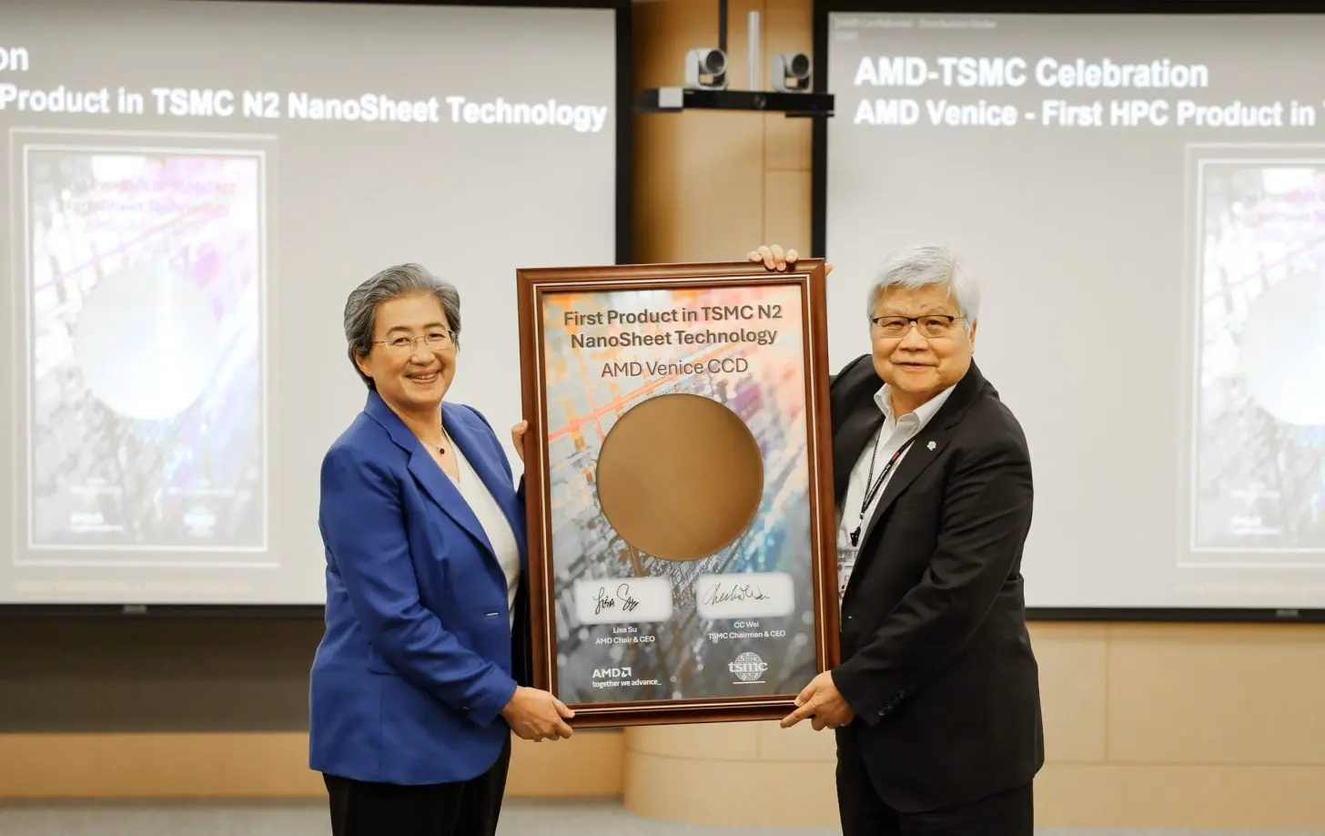
Source: wccftech.com



Discussion
0 comments
Log in to join the thread with a thoughtful take, question, or correction.