
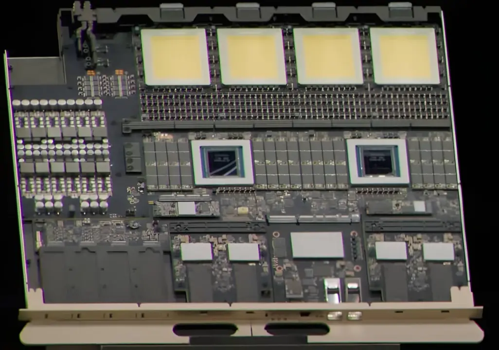
Nvidia to turn to (unlikely) PTFE to end key transmission choke point. Key note: The new gen "Rubin Ultra". Important: AI chips now hit a 200Gbps per lane that stresses the signal integrity of server boards.
NVIDIA explores PTFE for Rubin Ultra switch boards to address AI signal loss
What's the impact? Signal loss at these speeds hamper the efficiency of large AI compute clusters. What's going on?
Those in the industry, and engineers, are watching this. It hints at a change in the way high performance AI setups will be built.
What could be the possible (unlikely) solution Nvidia is eyeing up for this hardware issue? PTFE (aka Teflon for the brand). Why?
The idea is to integrate it in a Rubin Ultra switchboard or a new gen ortho mid-plane. Focus? The fundamental connectivity layer of the AI server where data is transferred between GPUs at breakneck speeds.
Turning point? Breaking away from using typical materials in current high-speed electronics.
Key part? PTFE loses much less of its signal energy (compared to what current board resins do). So there's less signal loss.
Problem? Top notch current M9 materials are not up to it when it comes to 70-plus layer boards. That's a performance difference.
Industry sources say: The retention of signal energy is much better with PTFE than with current epoxy / hydrocarbon resins. That tech benefit addresses a key weakness of current materials when it comes to handling high-frequency data flows.
But why? It's challenging to process PTFE because of bad bonding properties and its softness. Implications?
That makes it hard to manufacture. And? Overall yields are estimated to be below 5% by the industry.
So that's a big production issue. What about equipment? Industry partners in China / Taiwan / US have equipment in place to manage the PTFE processing.
What's needed? Engineering tweaks are needed to work around the physical limitations and enable large-scale production.
When? Roughly 2028-2030 before you see a clear result. Will PTFE become mainstream?
Probably not because of processing challenges and lack of belief (by manufacturers). And Nvidia is pushing on with this. But when will it be commercially viable?
A long way off. Industry is in long-term development mode to see if this material approach works and scales up.


teflon for servers is wild tbh 🤔
How much of that 200Gbps per lane loss is physical versus electrical noise? I want independent numbers on the 70 layer board yield drop.
The article states current M9 materials fall short at 70 plus layers. PTFE retains signal energy better than epoxy resins. The yield is the main issue at below 5 percent.
my desk is already full and i am still waiting for better ram prices not switch board materials
PTFE bonding is a nightmare for firmware calibration. Processing softness will likely cause micro-shifts in the mid-plane over time. Driver teams will hate this latency variance.
2028 is too far for current AI clusters to wait. I suspect they will stick with improved M9 and accept the loss rather than retooling factories for Teflon.