
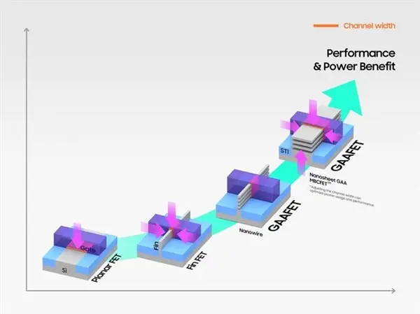
Samsung and SK Hynix are competing to define the architecture for seventh-generation DRAM, known as 1d. Both companies have presented their approaches at recent industry events. The two designs take different paths to improve density and performance.
Two competing architectures emerge
Samsung is promoting GAAFET technology for 7th gen DRAM. The company plans to present a 16-layer vertical stacked DRAM solution using GAA transistors at the 2026 VLSI Symposium. The design integrates the transistor and capacitor in the same cell. SK Hynix has adopted a 4F² architecture with vertical transistors. The capacitor sits below the transistor pillar. This 4F² design reduces chip area by about 30 percent compared to the conventional 6F² layout.
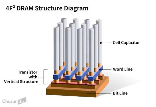
Samsung expects its vertical channel transistor products to launch in 2 to 3 years. SK Hynix plans to mass produce vertical DRAM with the 4F² architecture within 3 years.
Both companies are racing to set the standard for the next DRAM generation. Samsung's GAAFET approach uses horizontal capacitors and vertical stacking. SK Hynix's 4F² design relies on a vertical gate platform. The two strategies highlight different engineering trade-offs for scaling beyond current DRAM nodes.
The exact launch windows for commercial products remain unconfirmed by the vendors. Samsung and SK Hynix have not disclosed specific pricing or volume targets for their 7th generation DRAM.
Discussion
0 comments
Log in to join the thread with a thoughtful take, question, or correction.