
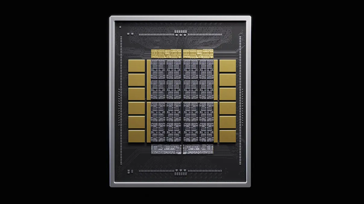
Nvidia has introduced NVHBM, a custom memory architecture designed to give AI chip makers a significant edge in bandwidth and efficiency. This shift matters because memory speed often bottlenecks AI inference performance, and NVHBM promises to unblock that constraint for developers using Nvidia's NVLink Fusion ecosystem. Buyers and engineers should care because this technology offers a path to faster token generation without increasing power draw.
Custom memory architecture boosts AI inference throughput
The core innovation lies in how NVHBM restructures the memory stack compared to standard HBM4e modules. Nvidia moved the memory controller from the main processor die into the base die of the HBM stack itself. This architectural change allows the use of a smaller custom PHY, which fundamentally alters how the memory interfaces with the compute silicon.
These structural adjustments yield measurable gains in both speed and silicon real estate. Nvidia states that NVHBM delivers up to 30% higher bandwidth per stack than commodity HBM4e. The company also claims the design consumes 15% less power than standard HBM4e equivalents. By offloading the controller, Nvidia frees up package real estate that can now support up to 30% more compute area on the primary silicon die.
The technology also aims to simplify the complex routing required for advanced packaging techniques. Nvidia claims the design simplifies interposer routing used to join multiple chips together. For memory-bandwidth-bound AI workloads, this higher bandwidth translates directly into higher throughput, such as a higher tokens-per-second rate for AI inference. Annapurna Labs, the chip unit behind Amazon's AWS infrastructure, is the first partner to adopt this approach.
Annapurna Labs VP Nafea Bshara stated, "We look forward to this technology collaboration to benefit future AWS infrastructure designs." While Annapurna's next-generation Trainium 4 chips will support the NVLink Fusion scale-up interface, the source notes it seems likely but not definitive that follow-on chips will support NVHBM. NVHBM is not a replacement for commodity HBM but serves as a building block for custom silicon developers looking to optimize their AI accelerators.
Discussion
0 comments
Log in to join the thread with a thoughtful take, question, or correction.