
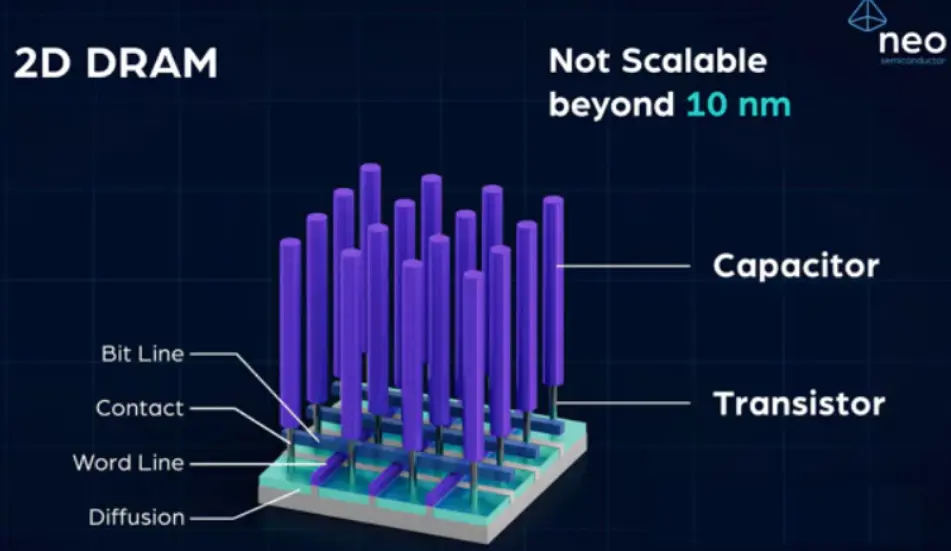
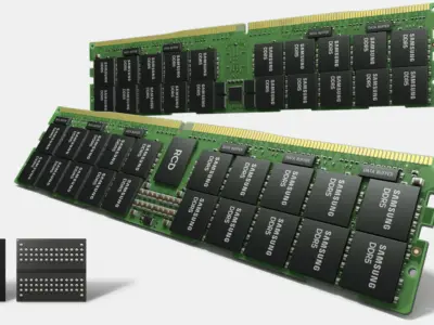
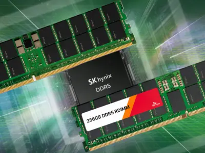
Samsung and SK Hynix are developing next-generation 3D DRAM manufacturing processes to overcome scaling limits below 10nm. Both companies aim to achieve mass production first and set their solution as the industry standard.
Samsung pursues GAAFET process for DRAM
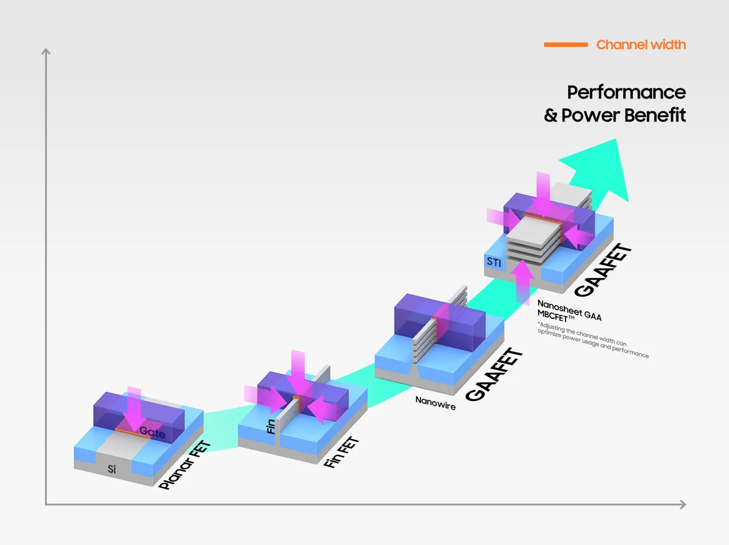
Samsung plans to promote a GAAFET process for DRAM, integrating GAAFET transistors with capacitors in the same cell. The company is considering a design similar to NAND flash, placing control circuits under the storage array.
SK Hynix adopts 4F2 architecture
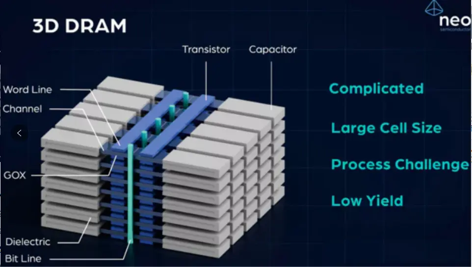
SK Hynix has chosen the 4F2 architecture, stacking transistors vertically with gate material wrapping the transistor. The component that receives capacitor data is placed beneath the transistor pillar.
The competition between Samsung and SK Hynix in 3D DRAM development is driven by the need for memory dominance in the AI era. According to Wccftech, both companies are vying to lead the next phase of DRAM technology.
Discussion
0 comments
Log in to join the thread with a thoughtful take, question, or correction.