
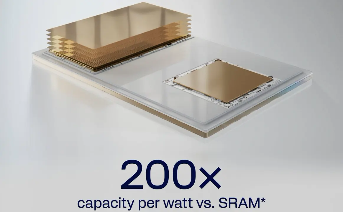
Qualcomm introduced High-Bandwidth Compute (HBC) to address the growing energy and speed bottlenecks in artificial intelligence data centers. This new architecture matters to buyers because it promises to significantly lower the total cost of ownership by reducing the energy required to process each AI token. The shift challenges the current industry standard of using High Bandwidth Memory (HBM) for high-performance computing tasks.
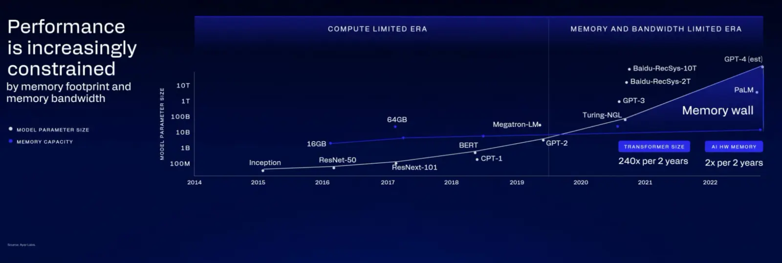
New stacked memory design targets AI data center efficiency
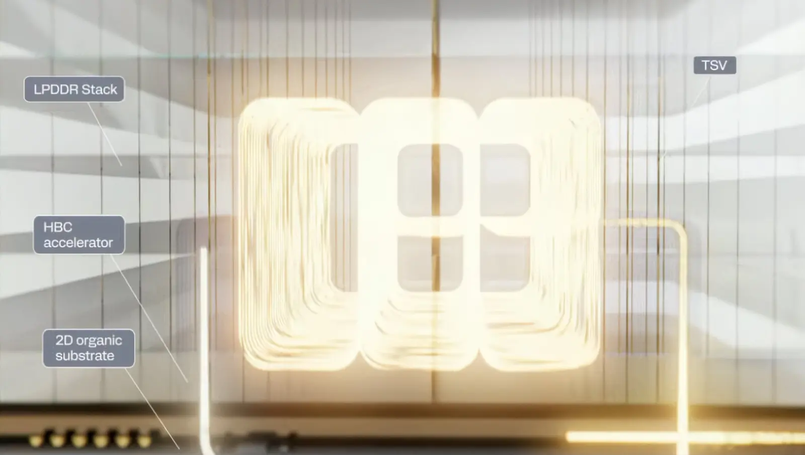
The core of the HBC design involves stacking LPDDR memory directly beneath the compute accelerator using Through-Silicon Vias (TSVs). This physical arrangement breaks the traditional memory wall by placing processing power closer to the data storage. Qualcomm plans to implement this first-generation HBC solution on its upcoming AI250 accelerator chip.
Spec comparison
| Spec | AI250 (Gen1) | AI300 (Gen2) |
|---|---|---|
| Bandwidth per card | 133 TB/s | N/A |
| Bandwidth per watt vs HBM | 6x increase | 7x jump |
| Effective bandwidth boost vs AI200 | 18x boost | 54x speed-up |
| Capacity per watt vs SRAM | 200x increase | N/A |
The AI250 accelerator delivers 133 terabytes per second of bandwidth per card. This specification represents an 18x boost over the previous AI200 model which relied on LPDDR5X memory. The HBC architecture provides a 6x increase in bandwidth per watt compared to standard HBM solutions. This efficiency gain allows for higher throughput without a proportional increase in power consumption.
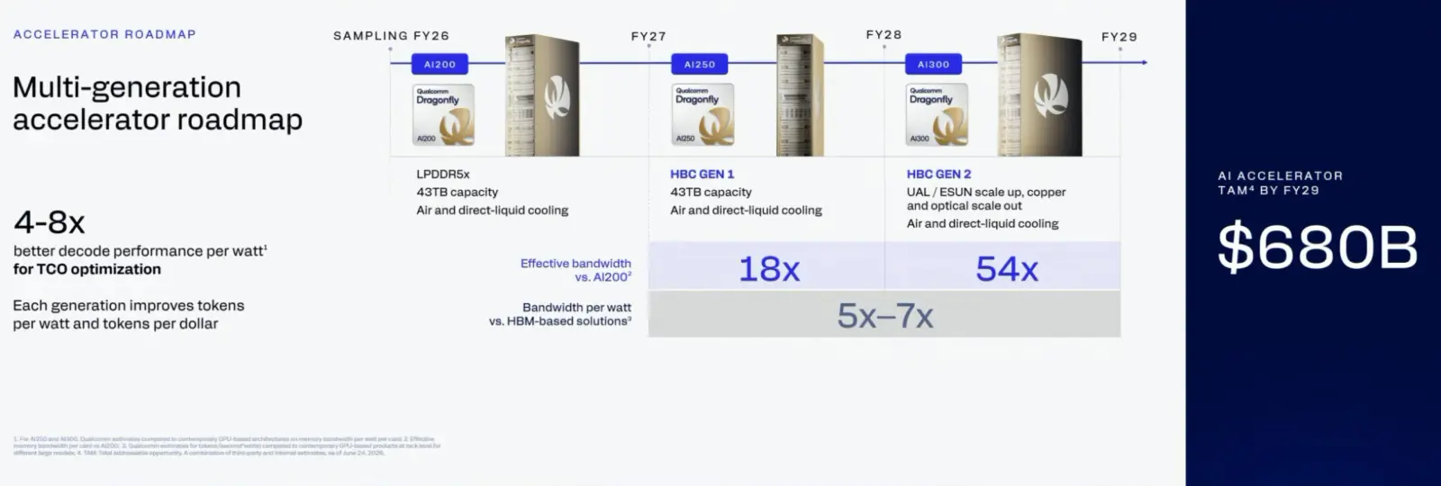
Qualcomm also outlined its second-generation HBC Gen2 solution, which will utilize the AI300 accelerator. The AI300 targets a 54x speed-up in effective bandwidth compared to the AI200 and offers a 7x jump in bandwidth per watt versus HBM. The company claims the 200x increase in capacity per watt versus SRAM further enhances the efficiency of this stacked memory approach.
The first-generation HBC Gen1 solution with the AI250 accelerators is expected to roll out globally by mid-2027. The second-generation HBC Gen2 solution for the AI300 is scheduled for release in 2028. These timelines place the technology in the near future for data center operators seeking to optimize AI workloads.
Qualcomm claims that the HBC architecture lowers the total cost of ownership compared to current HBM configurations. The design achieves this by providing lower energy input per token while increasing overall memory bandwidth. This approach offers a concrete path for reducing operational expenses in large-scale AI deployments.
Discussion
0 comments
Log in to join the thread with a thoughtful take, question, or correction.