
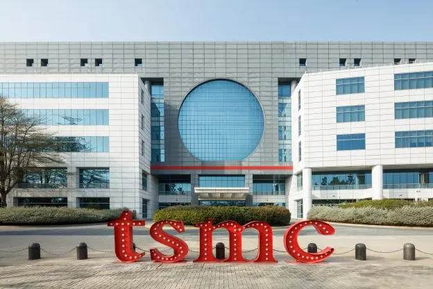
TSMC forecasts the global semiconductor market will exceed $1.5 trillion by 2030. The company expects AI and high-performance computing to account for 55% of that market. Smartphones will represent 20%, and automotive 10%.
AI and HPC to dominate 55% of market
To meet demand, TSMC plans to accelerate capacity expansion from 2025 to 2026. The company will add nine wafer fabs and advanced packaging facilities by 2026. Production capacity for 2nm and A16 chips will increase, with a compound annual growth rate of 70% from 2026 to 2028. CoWoS advanced packaging capacity is expected to grow at a CAGR of over 80% from 2022 to 2027. AI accelerator wafer demand is projected to increase 11 times from 2022 to 2026.
In Arizona, the first fab is operational. The second fab will begin equipment move-in in the second half of 2026. A third fab is under construction, and a fourth fab along with the first packaging facility will break ground this year. Arizona fab capacity is expected to grow 1.8 times year-over-year in 2026, with yields similar to those in Taiwan. TSMC has completed the purchase of a second large site in Arizona for future expansion. In Japan, the first fab is producing 22nm and 28nm chips, and the second fab has been upgraded to the 3nm process. The Germany fab is under construction, initially using 28nm and 22nm processes, later moving to 16nm and 12nm.
TSMC provided these forecasts and updates during its recent investor conference. The company has not confirmed specific timelines for all projects.

Discussion
0 comments
Log in to join the thread with a thoughtful take, question, or correction.