
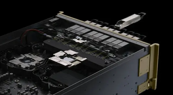
The AI chip industry is evaluating a new architecture to break the memory wall by separating GPU and HBM into independent packages.
New architecture places HBM several centimeters away from the GPU in a ring or central board area.
Optical interconnects will bridge data transmission between the separated modules.
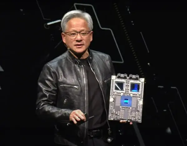
Current 2.5D packaging approaches face physical limits as GPU edge length restricts additional HBM placement.
HBM vertical stacking also nears its limit, with process complexity increasing exponentially beyond sixteen to twenty layers.
Discussion
0 comments
Log in to join the thread with a thoughtful take, question, or correction.