

The AI industry faces a critical bottleneck as memory bandwidth fails to keep pace with processing power. SanDisk has filed a patent for a new architecture designed to solve this specific problem. This development matters to buyers because it could lead to faster, more efficient AI hardware in the near future. The approach aims to reduce the distance data travels between memory and processors.
New architecture stacks memory directly under processors to ease AI bottlenecks
The core of this innovation is a 3D stacked chip architecture known as High-Bandwidth Flash. The design places a NAND Flash tile directly underneath a main compute tile, such as a GPU or AI accelerator. This vertical integration uses CMOS Bonded Array technology to connect the layers. The goal is to create a single unit that handles both storage and computation.
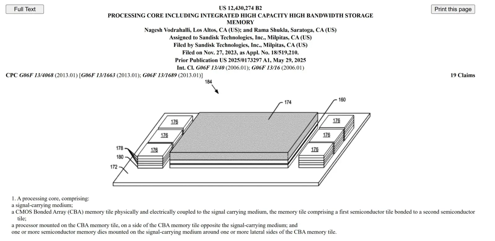
SanDisk holds US Patent 12,430,274 B2 for this configuration. The system uses Through Silicon Vias to stack NAND layers vertically. This method allows the stack to potentially reach capacities of 4 TB. The architecture combines high-capacity NAND with high-speed HBM DRAM on one interposer. This mix addresses the limitations of current standalone memory modules.
The patent establishes a strong strategic position for processor-on-NAND designs. Commercial products might initially use a simpler layout where components sit beside each other. This gradual approach allows manufacturers to refine the technology before full vertical integration. The filing signals a long-term shift in how AI chips manage data flow.



Discussion
0 comments
Log in to join the thread with a thoughtful take, question, or correction.