
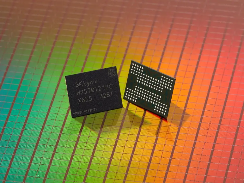
SK Hynix is adjusting its next-generation NAND flash roadmap. The company plans to use a 375-layer stacking design for its upcoming V10 product line instead of the originally targeted 400 layers. This change aims to reduce manufacturing complexity and improve yield rates during mass production. SK Hynix chose this design path to balance production feasibility with performance goals.
SK Hynix adjusts layer count to ease manufacturing complexity ahead of 2026 mass production.
The V10 NAND chip targets enterprise and high-end consumer storage markets. The company finished production validation and is preparing for mass production in 2026 via existing line upgrades. The company will integrate the design into existing manufacturing lines rather than building dedicated facilities. Using existing line upgrades allows SK Hynix to proceed with manufacturing without building new facilities.
Key specifications center on the layer count adjustment. The V10 NAND maintains a vertical stacking structure with 375 individual layers. SK Hynix cites production validation as complete for this specific configuration. The company plans to begin mass production in 2026 using upgraded existing lines.
Secondary details include the rationale behind the layer reduction. SK Hynix originally aimed for 400 layers but encountered scaling challenges during testing. The company selected 375 layers instead of the originally planned 400 to address mass production challenges. This approach supports a smoother transition to high-volume manufacturing compared to the initial design plan.
Pricing and specific product model names have not been disclosed at this time. The company has not yet announced retail prices or detailed model specifications for the V10 NAND. Current reports concentrate on production schedules and technical design details for the V10 NAND.
The decision reflects a common industry practice of adjusting design layers to ensure manufacturing stability. Other manufacturers often modify layer counts to handle similar manufacturing constraints. The V10 NAND is designed to advance storage density while maintaining production efficiency.
SK Hynix confirmed the 375-layer design choice through internal validation reports. Mass production is scheduled for 2026 via existing line upgrades. The company has not disclosed specific customer contracts or volume commitments at this stage.

Discussion
0 comments
Log in to join the thread with a thoughtful take, question, or correction.