
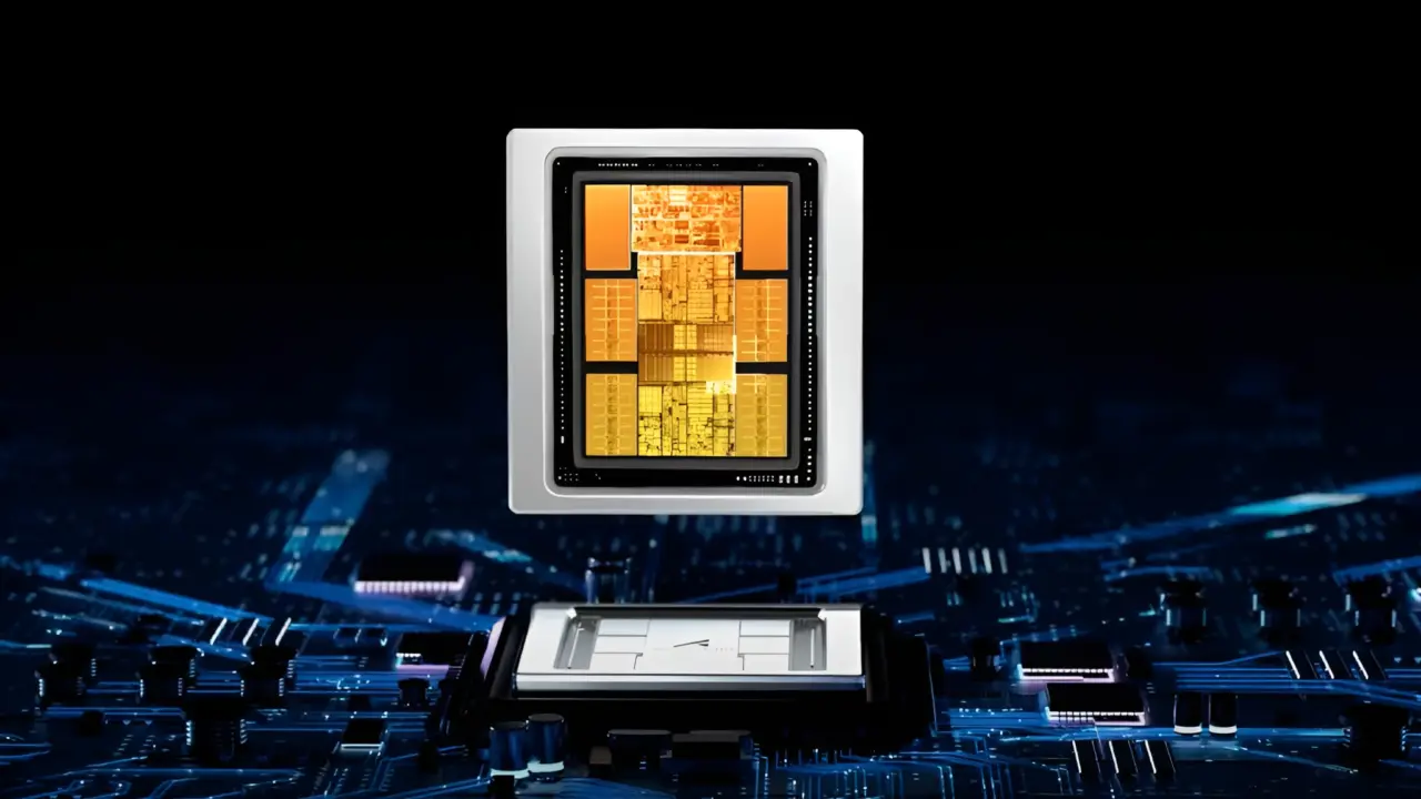
Huawei introduced Tau scaling technology, a research initiative aimed at achieving transistor densities equivalent to 14A process nodes. The announcement highlights the company's efforts to advance semiconductor manufacturing capabilities despite ongoing restrictions on access to extreme ultraviolet (EUV) lithography equipment.
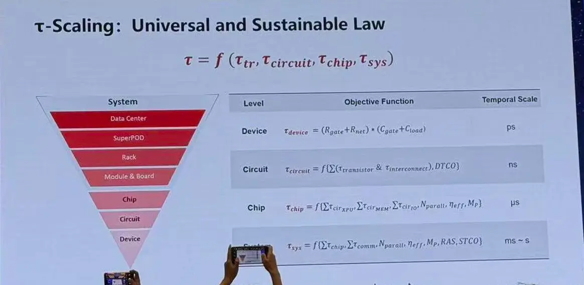
Expert analysis questions the practical performance benefits of Huawei's new logic-on-logic stacking technology
The core of Huawei's approach involves logic-on-logic stacking, which Dr. Ian Cutress describes as a form of 3D stacking. This method places logic gates directly atop other logic gates rather than combining them with SRAM memory components. The company claims to have achieved a pitch distance of two microns between these stacked layers.
Industry experts note that hybrid bonding and logic-on-logic concepts are not new, having been explored by major competitors like Intel and AMD for several years. Cutress acknowledges that Huawei's reported two-micron pitch represents a significant technical achievement in terms of density. However, he questions the practical performance benefits of this specific stacking configuration compared to traditional methods.
The announcement has drawn criticism regarding its framing of performance metrics. Cutress argues that Huawei is redefining industry standards for chip performance due to limitations imposed by US sanctions. He suggests the company's claims may be comparing unrelated technical specifications to create a more favorable impression of their progress.
Further scrutiny comes from observations about the research paper itself. Cutress pointed out stylistic indicators such as short sentences and translation errors that suggest artificial intelligence involvement in its creation. These details have led some experts to question the originality and rigor of the published findings.
Huawei continues to pursue advanced packaging techniques as a workaround for manufacturing constraints. The company's focus on logic-on-logic stacking represents one strategy to maintain competitiveness in semiconductor density without EUV tools. The semiconductor industry will track if Huawei's theoretical advancements can be successfully developed for commercial use.


Discussion
0 comments
Log in to join the thread with a thoughtful take, question, or correction.