
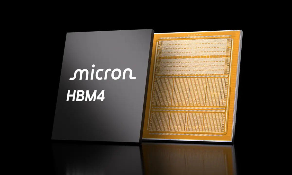
JEDEC has approved the SPHBM4 standard, a move designed to lower the manufacturing costs of high-bandwidth memory for AI and GPU hardware. This new specification allows memory modules to use standard substrates instead of expensive advanced packaging structures. Buyers and system builders will eventually see reduced hardware costs as the industry shifts away from complex fabrication methods. The change addresses a major bottleneck in producing the memory chips that power modern data centers and high-end graphics cards.
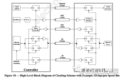
New standard reduces signal pins to one-fifth while quadrupling speed
The SPHBM4 standard, or Standard Package HBM4, defines how memory connects to compute dies in large-scale packages. It targets the same performance levels as the existing HBM4 specification but changes the physical interface. JEDEC created this standard to ensure that memory manufacturers can maintain high speeds without relying on costly production techniques. The specification positions itself as a bridge between current high-performance memory needs and more economical manufacturing realities.
SPHBM4 Key Specifications
- Signal Pin Reduction: 1/5th of HBM4 count
- Signal Speed Increase: Fourfold vs HBM4
- Die-to-Memory Distance: 20mm
- Substrate Compatibility: Standard substrates
The technical core of SPHBM4 involves a significant reduction in the number of signal pins required for operation. The standard cuts the pin count to one-fifth of the HBM4 requirement, which drops from approximately 2,000 pins. To compensate for fewer connections, the signal speed increases fourfold compared to the 11Gbps baseline of HBM4. This higher speed ensures that the memory maintains HBM-class bandwidth despite the simplified physical layout.
SPHBM4 also increases the distance between the memory and the compute die to 20mm. This extra spacing improves internal thermal management by allowing heat to dissipate more effectively within the package. The standard is designed to work with emerging glass substrate technologies, which are expected to support large-scale package implementations. An industry insider noted that this combination enables the more economical placement of HBM-class memory in future devices.
Commercial availability for SPHBM4-based products remains distant as the underlying substrate technology is still in development. Trial production of glass substrates is expected in the coming years, with true commercialization anticipated around 2030. Until that time, manufacturers will continue using current packaging methods for HBM4 memory. The approval of SPHBM4 sets the technical roadmap for the next generation of memory hardware but does not immediately impact current supply chains.
Discussion
0 comments
Log in to join the thread with a thoughtful take, question, or correction.