
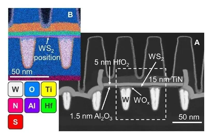
imec, ASML, and TSMC have demonstrated a scalable integration route for 2D-material transistors on standard 300 mm wafers. The collaboration achieved a contacted poly pitch of 50 nm without degrading device performance. This milestone addresses the traditional scaling bottleneck where smaller transistor channels require larger contact areas to maintain low resistance.
Collaboration demonstrates scalable manufacturing for next-gen semiconductor components
The research team utilized transition metal dichalcogenide materials for the transistor channels. They implemented molybdenum disulfide for n-type field-effect transistors and either tungsten disulfide or tungsten selenide for p-type devices. The process relied on single-patterning extreme ultraviolet lithography to define features at 28 nm channel lengths.
Electrical testing confirmed that both transistor polarities turn off completely when the gate voltage reaches zero volts. The wafers showed a 94% operational rate, defined by an on-current to off-current ratio exceeding 10^5. These results indicate that the manufacturing process yields functional devices at scale rather than isolated lab samples.
pFETs using tungsten selenide channels performed close to record levels seen in previous laboratory-based experiments. imec researchers stated this progress helps de-risk the transition from research labs to semiconductor fabrication facilities. The work establishes a foundation for future high-density logic architectures beyond current silicon limits.


Discussion
0 comments
Log in to join the thread with a thoughtful take, question, or correction.